ASML Ships Twinscan NXT:2000i Scanner for 7nm and 5nm DUV
by Anton Shilov on August 2, 2018 1:00 PM EST- Posted in
- Semiconductors
- EUV
- ASML
- DUV
- Twinscan NXT
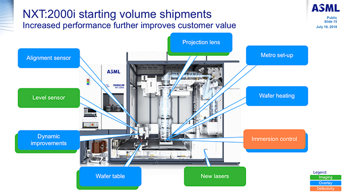
ASML, the company known for producing equipment for the manufacture of processors and semiconductors at foundries, has started to ship its new Twinscan NXT:2000i DUV (Deep Ultra Violet) scanner that matches overlay performance of the company’s Twinscan NXE:3400B EUV (Extreme Ultra Violet) scanner. The new machine will be used to make chips using 5 nm and 7 nm nodes and will be required by makers of semiconductors who will have tighter overlay requirements and will have to mix-and-match overlay capabilities between different types of step-and-scan systems.
When leading manufacturers of chips start to use Twinscan NXE EUV lithography scanners for their 7 nm and more advanced process technologies in the coming quarters/years for some of the metal layers for the processors, DUV equipment is still required for other layers (for example, GlobalFoundries first version of 7nm is DUV only). Different makers of semiconductors will have their own specific requirements for their 7 nm and 5 nm process technologies particularly when it comes to on-product as well as mix-and-match overlay capabilities.
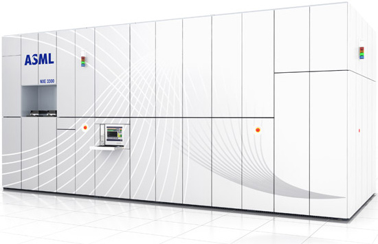
An example setup of a TwinScan NXE:3300-series EUV machine. It's quite big
Being a producer of step-and-scan systems, ASML develops equipment with generic requirements in mind: for a 7 nm node there is an on-product overlay requirement of 3.5 nm, so scanners have to support an overlay budget of 2.5 nm. Such requirements are achievable on ASML’s Twinscan NXE:3350B as well as the NXT:1980D tools. For 5 nm nodes overlay requirements will be tighter: ASML says that it is working with an on-product overlay requirement of 2.4 nm, which means that its scanners will have to feature an overlay budget of 1.9 nm. This numbers have been achieved by the NXE:3400B as well as the NXT:2000i machines.
Not all makers will need to match overlay accuracy across different step-and-scan systems, but those who will are going to need the new Twinscan NXT:2000i DUV scanners to work with the NXE:3400B EUV tools. The new systems do not necessarily offer a higher wafer throughput when compared to the NXT:1980D, but feature “several hardware innovations that will enable on-product overlay of 2.5 nm in mix-and-match use with EUV for the 7 and 5 nanometer logic nodes.”
ASML started volume shipments of its new Twinscan NXT:2000i step-and-scan systems last quarter and will ramp up production of the new tools in the coming years. Traditionally, the company does not disclose MSRPs of its equipment as final prices depend on multiple factors, including volumes.
Related Reading
- Samsung Foundry Roadmap: EUV-Based 7LPP for 2018, 3 nm Incoming
- Arm and Samsung Extend Artisan POP IP Collaboration to 7LPP and 5LPE Nodes
- The Future of Silicon: An Exclusive Interview with Dr. Gary Patton, CTO of GlobalFoundries
- EUV Lithography Makes Good Progress, Still Not Ready for Prime Time
- GlobalFoundries Gives 7 nm Capacity Update, Mulls Skipping 5 nm
Source: ASML


15 Comments
View All Comments
edzieba - Friday, August 3, 2018 - link
... What do you think Intel have been doing for the past few years? 14+, 14++ and 14+++ are exactly that, just without the "decrement the number and pretend it's a whole new process" schtick.SquarePeg - Friday, August 3, 2018 - link
This isn't what Samsung has been doing. All of Intel's +++'s together only equal a half node process improvement and density actually decreased from OG 14nm to 14nm+. Samsung has been on a steady cadence of density increases one year and power performance improvement the next since they moved on from 28nm. Though each Samsung "tick tock" is smaller in size than Intel's major process shrinks. But then again Intel's been stuck on the same node for what will be 5 years.For a quick look at what's actually been going on here a link.
https://www.anandtech.com/show/12096/samsung-start...
Santoval - Monday, August 6, 2018 - link
Their first non monolithic chips are the new -AP series of Cascade Lake, its successor Cooper Lake and then (in 2H 2020) of Ice Lake. These will be their top-end, cutting edge CPUs, above even their current top-end SP series. They could employ any number and type of dies in them, from two 10-core dies for a 20-core package (which is cheaper than a 20-core -SP CPU with a monolithic die), to four 28-core dies for a.. 112-core package, maybe trimmed to 110 cores (with *severe* underclocking), or any other combination between these two extremes.They will use EMIB to "glue" the dies, which is faster than AMD's Infinity Fabric and places all dies at the edge of each other, with no space between them. That trims the area of the package, but it also worsens the effects of high TDPs, since the "TDP density" (active heat per mm^2) is higher, while the neighbouring inactive dies are exposed to more heat by the active ones compared to AMD's Epyc. Currently Intel have no plans for multi-die packages for their consumer CPUs, not even for the HEDT ones (the -X series). At least they have announced none.
psychobriggsy - Tuesday, October 23, 2018 - link
You can't compare EMIB to Infinity Fabric. One is physical, the other is a protocol. That protocol could run over an interposer or EMIB, and in doing so it could be made wider, faster and lower-power, as that is what those physical interfaces allow.psychobriggsy - Tuesday, October 23, 2018 - link
I suspect that there is some truth in the 10nm cancellation rumour, but that Intel have something lined up to replace it, maybe a bit later, that they will call 10nm. It's probably not as good in terms of density. If anything emerges in 2019 then it'll be the Y and U series IceLakes, but anything interesting will be 2020.Intel has done minor tweaks to the 14nm process, sure, but they're not half-node shrinks. They're optimisations and tweaks for higher power usage in order to get higher clocks.