NVIDIA Develops NVLink Switch: NVSwitch, 18 Ports For DGX-2 & More
by Ryan Smith on March 27, 2018 1:20 PM EST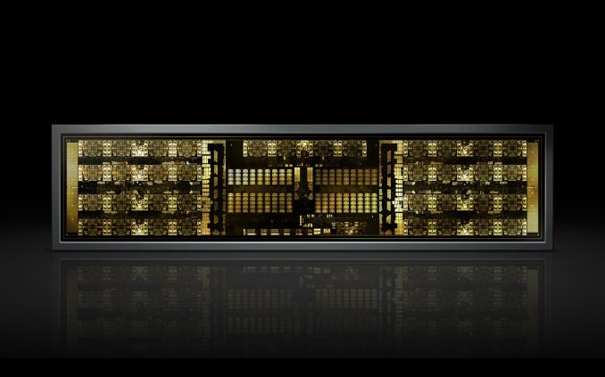
Back in 2016 when NVIDIA launched the Pascal GP100 GPU and associated Tesla cards, one of the consequences of their increased server focus for Pascal was that interconnect bandwidth and latency became an issue. Having long relied on PCI Express, NVIDIA’s goals for their platform began outpacing what PCIe could provide in terms of raw bandwidth, never mind ancillary issues like latency and cache coherency. As a result, for their compute focused GPUs, NVIDIA introduced a new interconnect, NVLink.
With 4 (and later 6) NVLinks per GPU, these links could be teamed together for greater bandwidth between individual GPUs, or lesser bandwidth but still direct connections to a greater number of GPUs. In practice this limited the size of a single NVLink cluster to 8 GPUs in what NVIDIA calls a Hybrid Mesh Cube configuration, and even then it’s a NUMA setup where not every GPU could see every other GPU. Past that, if you wanted a cluster larger than 8 GPUs, you’d need to resort to multiple systems connected via InfiniBand or such, losing some of the shared memory and latency benefits of NVLink and closely connected GPUs.
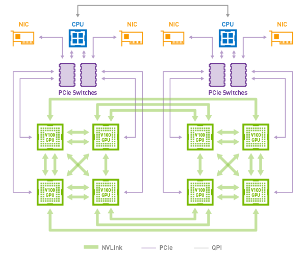
8x Tesla V100s in a Hybrid Mesh Cube Topology
For practical reasons, going with an even larger number of NVLInks on a single GPU is increasingly impractical. So instead NVIDIA is doing the next best thing – and taking the next step as an interconnect vendor – by producing an NVLink switch chip.
The switch, aptly named NVSwitch, is designed to enable clusters of much larger GPUs by routing GPUs through one or more switches. A single switch has a whopping 18 full-bandwidth ports – three-times that of a GV100 GPU – with all of the ports in a fully connected crossbar. As a result a single switch has an aggregate of 900GB/sec of bidirectional bandwidth.
The immediate goal with NVSwitch is to double the number of GPUs that can be in a cluster, with the switch easily allowing for a 16 GPU configuration. But more broadly, NVIDIA wants to take NVLink lane limits out of the equation entirely, as through the use of multiple switches it should be possible to build almost any kind of GPU topology. Consequently the NVSwitch is something of a “spare no expense” project for the company; this is embodied by the transistor count of the chip, which weighs in at around 2 billion transistors. This makes it larger than even NVIDIA’s entry-level GP108 GPU, and considering this is just for a switch, all of this amounts to somewhat crazy number of transistors.
Unfortunately while NVIDIA has announced the bandwidth numbers for the NVSwitch, they aren’t yet talking about latency. The introduction of a switch will unquestionably add latency, so it will be interesting to see just what the penalty is like. Staying on-system (and with short traces) means it should be low, but it would diminish the latency advantages of NVLink somewhat. Nor for that matter have power consumption or pricing been announced.
DGX-2: 16 Tesla V100s In a Single System
Unsurprisingly, the first system to ship with the NVSwitch will be a new NVIDIA system: the DGX-2. The big sibling to NVIDIA’s existing DGX-1 system, the DGX-2 incorporates 16 Tesla V100 GPUs. Which as NVIDIA likes to tout, means it offers a total of 2 PFLOPs of compute performance in a single system, albeit via the more use-case constrained tensor cores.

NVIDIA hasn’t published a complete diagram of the DGX-2’s topology yet, but the high level concept photo provided indicates that there are actually 12 NVSwitches (216 ports) in the system in order to maximize the amount of bandwidth available between the GPUs. With 6 ports per Tesla V100 GPU, this means that the Teslas alone would be taking up 96 of those ports if NVIDIA has them fully wired up to maximize individual GPU bandwidth within the topology.

Notably here, the topology of the DGX-2 means that all 16 GPUs are able to pool their memory into a unified memory space, though with the usual tradeoffs involved if going off-chip. Not unlike the Tesla V100 memory capacity increase then, one of NVIDIA’s goals here is to build a system that can keep in-memory workloads that would be too large for an 8 GPU cluster. Providing one such example, NVIDIA is saying that the DGX-2 is able to complete the training process for FAIRSeq – a neural network model for language translation – 10x faster than a DGX-1 system, bringing it down to less than two days total.
Otherwise, similar to its DGX-1 counterpart, the DGX-2 is designed to be a powerful server in its own right. We’re still waiting on the final specifications, but NVIDIA has already told us that it’s based around a pair of Xeon Platinum CPUs, which in turn can be paired with up to 1.5TB of RAM. On the storage side the DGX-2 comes with 30TB of NVMe-based solid state storage, which can be further expanded to 60TB. And for clustering or further inter-system communications, it also offers InfiniBand and 100GigE connectivity.
| NVIDIA DGX-2 Specifications | |||
| CPUs | 2x Intel Xeon Platinum (Skylake-SP) | ||
| GPUs | 16x NVIDIA Tesla V100 | ||
| System Memory | Up To 1.5 TB DDR4 (LRDIMM) | ||
| GPU Memory | 512GB HBM2 (16x 32GB) | ||
| Storage | 30TB NVMe, Upgradable to 60TB | ||
| Networking | 8x InfiniBand EDR/100GigE | ||
| Power | 10,000 Watts | ||
| Size | ? | ||
| GPU Throughput | FP16: 480 TFLOPs FP32: 240 TFLOPs FP64: 120 TFLOPs Tensor (Deep Learning): 1.92 PFLOPs |
||
Ultimately the DGX-2 is being pitched at an even higher-end segment of the deep-learning market than the DGX-1 is. Priced at $399K for a single system, if you can afford it (and can justify the cost) you’re probably Facebook, Google, or in the same league thereof.


22 Comments
View All Comments
mode_13h - Friday, March 30, 2018 - link
Ah, but for all those negatives, it's doing two things for them.1. Moving a lot of GPUs. This translates into revenue they can re-invest in their product stack.
2. Pushing customers towards higher-margin Quadro and Tesla solutions, which turns into even more revenue.
I think any tears he may shed over crypto are most definitely crocodile tears. They might view it as problematic, but it's sure a high-class problem to have.
Yojimbo - Friday, March 30, 2018 - link
1. NVIDIA has plenty of cash and profits. Their long term markets are more important2. How many people are buying a Quadro or a Tesla instead of a GeForce?
Certainly NVIDIA loves more demand, but they don't want volatile demand. They also don't want current generation cards coming back into the market if there is a crypt crash. Another headache. NVIDIA is doing just fine without crypto. They really don't need it strengthening AMD's research budget, disrupting their market visibility, and especially they don't need it to push gamers away from PC gaming.
Dug - Tuesday, March 27, 2018 - link
I don't know anything about the gpu, but I want to know more on how it handles the 30TB of NVMe-based solid state storage. Is it a custom controller or interface and does it run off of the pci-e?Ryan Smith - Tuesday, March 27, 2018 - link
If it's anything like the DGX-1, then it's just multiple SSDs in a single system.Elstar - Tuesday, March 27, 2018 - link
30 TB is not a lot for a box this expensive and this complicated. It is probably just plain NVMe.The Hardcard - Tuesday, March 27, 2018 - link
What is the TDP for pumping 900 GB/s. Liquid cooling I presume?mode_13h - Wednesday, March 28, 2018 - link
One of the slides says "3,200 Watts of maximum system power" in 3U.Yojimbo - Wednesday, March 28, 2018 - link
I don't think it has liquid cooling. Here's a picture of it pulled apart: https://images.anandtech.com/doci/12587/screenshot...Each NVSwitch is 2 billion transistors. So I imagine the power draw of the switch fabric is not insignificant. I really have no idea how it works but I'm just going to through out a guess anyway. I'd imagine that a switch fabric would be less efficient than NVLink. NVLink 2 allows 300 GB/s bi-directional throughput and NVLINK-enabled GPUs have 50 W higher TDP. I have no idea if it at all makes sense to figure it this way, but if NVSwitch is less efficient and allows 900 GB/s bi-directional throughput then the TDP of one switch should be over 150 W. The DGX-2 has 12 NVSwitches, so that would be 1800 W of TDP for the NVSwitch fabric in the DGX-2. Of course, maybe there is some power savings as some of the NVLink power usage on the GPUs is shifted to the switch when the fabric is used? Real world power usage would depend a lot on how much cross GPU communications can be kept down, of course.
Yojimbo - Wednesday, March 28, 2018 - link
Or maybe the switch itself doesn't see that sort of power usage because a lot of the power overhead is still taken up by the NVLink on the GPU. Either way, the power cost of using all that bandwidth is significant compared to if you had 16 GPUs that couldn't talk to each other, or only did so slowly.Yojimbo - Wednesday, March 28, 2018 - link
The TDP of 16 non-NVLink V100s is 250 W, BTW. So 16 of them would be 4,000 W TDP. Could the use of this switch really raise TDP by 45% to 5,800 W? Got me... You also have to consider the power savings from the PCI Express switches that your are replacing.