TSMC Starts to Build Fab 18: 5 nm, Volume Production in Early 2020
by Anton Shilov on January 31, 2018 2:00 PM EST- Posted in
- Semiconductors
- SoCs
- EUV
- TSMC
- 5nm
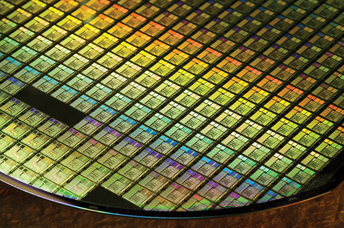
TSMC last week held a groundbreaking ceremony for its Fab 18 phase 1 production facility. The fab will produce chips using TSMC’s 5 nm process starting from early 2020. When all three phases of the manufacturing facility are completed, its wafer starts capacity will exceed one million 300-mm wafers per year, comparable with other three GigaFabs operated by TSMC.
TSMC’s Fab 18 will be located in Tainan (in the Southern Taiwan Science Park), and will be built in three phases. The construction of the first phase or segment of the building will be completed in about a year from now, after which TSMC will move in equipment sometime in early 2019. In about two years from now, the company expects to start volume production of chips using its 5 nm process technology at the Fab 18/phase 1. Construction of the second and the third phases will commence in Q3 2018 and Q3 2019. The two phases will start volume production in 2020 and 2021, respectively.
| TSMC's Fab 18: Milestones | |||||
| Phase 1 | Phase 2 | Phase 3 | |||
| Construction Start | Early 2018 | Q3 2018 | Q3 2019 | ||
| Equipment Move-In | Early 2019 | ? | ? | ||
| High-Volume Manufacturing Start | Early 2020 | 2020 | 2021 | ||
The Fab 18 will have a total floor area of 950,000 square meters and its cleanroom area will exceed 160,000 square meters, the contract maker of semiconductors said. TSMC estimates that the combined production capacity of all three phases of the Fab 18 will exceed one million 300-mm wafer starts per year, which is comparable to the capacities of the other GigaFabs that TSMC operates — Fab 12, Fab 14, and Fab 15. It is noteworthy that the planned floor area and cleanroom space of the Fab 18 will be significantly larger than the initially planned floor and cleanroom area of the Fab 15, which emphasizes increasing complexity of IC manufacturing these days as well as increasing orders from TSMC's clients. In total, the Fab 18 will cost TSMC NT$500 billion ($17.08 billion), making it one of the most expensive chip manufacturing facilities in the world.
| Brief Comparison of TSMC's Fab 15 and Fab 18 | ||||
| Fab 15 | Fab 18 | |||
| Total Area of Site | 18.4 hectares | ? | ||
| Building Area | 430,000 m² | 950,000 m² | ||
| Clean Room Space* | 104,000 m² | 160,000 m² | ||
| Initially Expected Investment** | NT$300 billion ~$9.375 billion |
NT$500 billion ~$17.08 billion |
||
| Groundbreaking | July 2010 | January 2018 | ||
| Notes | *Fabs are usually upgraded over time, today's cleanroom space of the Fab 15 may be larger than initially projected. **Initially expected investments tend to change over time. |
|||
Besides its dimensions and cost, there is another reason why Fab 18 is important for the semiconductor industry: it will be one of the world’s first facilities to produce chips using a 5-nm production tech. TSMC yet has to detail its 5 nm manufacturing technology, but from the announcements that the company has made so far it is evident that this fabrication process will rely significantly on EUV lithography. TSMC did not mention EUV at all in its press release, which is a bit strange. Meanwhile, over the course of last year the semiconductor manufacturer did mention that the 5 nm fabrication technology would be its second-gen EUV process, which means usage of EUV for more more layers when compared to the CLN7FF+ (its advanced 7 nm tech). Furthermore, TSMC already has functional SRAM cells made using its CLN5FF technology and the yields were satisfactory in mid-2017. Therefore, the 5 nm development process seems to be going on relatively well.
The extended usage of EUV for 5-nm chip production means that the company will need to install more EUV tools into the Fab 18, which is one of the reasons why it needed to expand the fab’s cleanroom space. The fact that TSMC has begun to build Fab 18 indicates that the contract maker of chips is confident in its 5 nm technology as well as EUV equipment, including ASML’s TWINSCAN NXE scanners, Cymer’s EUV light sources and other tools. This confidence is further underscored by their intention to start high-volume manufacturing of 5-nm devices in Fab 18 in early 2020.
| Advertised PPA Improvements of TSMC's CLN7FF Nodes Data announced by TSMC during conference calls, press briefings and in press releases |
||||||
| 7FF vs 16FF+ |
7FF vs 10FF |
7FF EUV vs 7FF |
5FF EUV vs 7FF EUV |
|||
| Power | 60% | <40% | 10% | lower | ||
| Performance | 30% | ? | lower | higher | ||
| Area Reduction | 70% | >37% | ~10% | tangible | ||
| HVM Start | ~Q2 2018 | - | ~H2 2019 | H1 2020 | ||
Related Reading:


26 Comments
View All Comments
HStewart - Wednesday, January 31, 2018 - link
This whole nm size stuff reminds me of days of Frequency wars back in Pentium 4 days - but sort of in reverse. We are actually not sure exactly what Intel's 10nm is like - but it like be more dense that other processes significantly. This is why it taking longer get out. I believes Intel's process is 3D process.In any case, what matters is how many transistors / components can be in square area and not nm metric.
Most exiting thing about Intel's processes is that it can combine multiple processes on the same die. This means important components like CPU / GPU / Memory can be on denser material why the IO and less important components can be done on less denser. I don't believe Intel is using this for combo Intel CPU / AMD GPU component - that things reminds me of last Celeron / Pentium components - which have more in common with Atom that higher level processors. I was frustrated with my Lenovo 100s 14in - I could not update memory.
I hope none of my comments have mistakes - because I wish we could edit comments here.
Wilco1 - Thursday, February 1, 2018 - link
"In any case, what matters is how many transistors / components can be in square area and not nm metric."7nm TSMC density is 116 million transistors/mm^2, while Intel 7nm does ~100. See https://www.semiwiki.com/forum/content/6713-14nm-1...
"I hope none of my comments have mistakes"
Well pretty much all of our post is FUD or fake news as it is called nowadays. Combining multiple processes on the same die? 3D process? What pills did you take?
Santoval - Thursday, February 1, 2018 - link
I checked out the article you linked and apparently I was wrong above. It says Samsung's 7nm is going to have 127.3 MTr/mm^2 and TSMC's 7nm will have 116.7 MTr/mm^2. I had no idea they were so ambitious. Since Intel will retain 10nm for at least three CPU generations I will concede that they have fallen behind Samsung and TSMC (and GloFo?) even if the others' 7nm node is released two, three or even four quarters after Intel's 10nm.MrSpadge - Thursday, February 1, 2018 - link
" We are actually not sure exactly what Intel's 10nm is like - but it like be more dense that other processes significantly. This is why it taking longer get out. I believes Intel's process is 3D process."They've published details at conferences. FinFETs (in that sense as 3D as before) with air gaps to reduce capacitance and increase performance, together with a material change for the Vias, if I remember correctly. That's quite ambitous and will give them an advantage over processes without those changes.
Density figures have also been published: more dense than TSMCs & Samsungs 10 nm, but less dense than competing 7 nm processes.
FullmetalTitan - Thursday, February 1, 2018 - link
Everyone else covered the wealth of density info released over the last 2 years."Most exiting thing about Intel's processes is that it can combine multiple processes on the same die. This means important components like CPU / GPU / Memory can be on denser material why the IO and less important components can be done on less denser."
This is just local pattern density? You can make transistors larger or less dense than the half-pitch node naming implies.
" I don't believe Intel is using this for combo Intel CPU / AMD GPU component..."
No idea what this rambling means, but Intel is just packaging a coffee lake CPU with a custom Vega die and HBM2 for easier integration into ultrabooks and such, there is nothing special about that venture.
Dragonstongue - Wednesday, January 31, 2018 - link
TSMS/GF/Samsung/IBM etc all build their wafer much differently than Intel does, so, a problem that affects one does not automatically mean it effects the others.I have a feeling Intel was "milking it" because for years and years no other fab was close to competing with them being "the most advanced" so they did as little as they possibly could to ensure the lowest cost highest ROI on every chip/product they sold, but since 28nm, now 14-12-7nm soon enough the competition caught up quite quickly.
Intel may be the "leading producer" but, they generally only produce their own chips, so someone like TSMC whos only job is to build for others gets $ from many places and does many different designs as well, so at least in my opinion, this gives them maybe that much more ability to "tweak" their designs going forward, so in theory would mean more flexibility to work through or around kinks that maybe Intel cannot.
Generally because of the way Intel builds their "bulk" transistors it allows them to have far tighter tolerance on gates and the like, so more oft than not means less voltage required for higher speed or at very least more density per die, this is something that gave them a major advantage vs others (generally using SOI or FD-SOI) however, the density, transistor count, leakage and so forth of Intel vs competition (TSMC-Samsung/GF/IBM) has been very much eroding over the last decade.
So just to iterate IMO just because Intel got lazy or screwed up however you want to word it, they still are making $$$$$$$$$ and really only produce chips for their own purpose, so they likely do not have nearly the same motivation at keeping at the absolute bleeding edge when it comes to nm scaling like they once did, am sure they have many other fish in the pot to worry about.
TSMC as an example, only job is to produce the chips they are paid to do, so they have every motivation to keep pushing in lowever nm higher density, if they are not "the best" others will be, means less $$$$ Intel still makes loads of $$$ from being able to produce high density chips AND making the chips as well.
anyways ^.^
HStewart - Wednesday, January 31, 2018 - link
"Intel may be the "leading producer" but, they generally only produce their own chips, so someone like TSMC whos only job is to build for others gets $ from many places and does many different designs as well"One thing to remember that could be key to future Intel processes is that Intel purchase Altlera which is/was a leader in maker of "Field Programmable Gate Array" which is used to create custom design logic for many different purpose. This was done a while back and I believe a lot of Intel's future designed will benefit from this purchase. This purchase likely means that Intel process will be open to others.
FullmetalTitan - Thursday, February 1, 2018 - link
Intel lost their status as "leading producer" last year. They have been floundering for a while. Ask anyone in the mfg environment and they will tell you that Intel talent has been fleeing for greener pastures for a while nowname99 - Thursday, February 1, 2018 - link
Uhhh, wot?One of these companies has made a habit of lying ever since the 14nm Broadwell delays.
And one has delivered on time year after year since at least 28nm.
Just because INTC doesn’t know what the hell they are doing doesn’t mean the rest of the world is as incompetent...
Lolimaster - Thursday, February 1, 2018 - link
Those are intel problems. global foundries is on track with 7nm.