The Intel Skylake-X Review: Core i9 7900X, i7 7820X and i7 7800X Tested
by Ian Cutress on June 19, 2017 9:01 AM ESTThe Basin Falls Platform: X299, SKL-X, & KBL-X
For most practical definitions of the Basin Falls platform, the X299 chipset is the heart. X299 supports the new processors, and like the Z170 and Z270 counterparts on the mainstream consumer line, is basically a big PCIe switch. One of the issues with the older X99 chipset was its limited capabilities, and inability to drive many PCIe devices – this changes with the big switch mentality on X299. For the DMI 3.0 link going into the chipset (basically a PCIe 3.0 x4), the chipset has access to up to 24 PCIe 3.0 lanes for network controllers, RAID controllers, USB 3.1 controllers, Thunderbolt controllers, SATA controllers, 10GbE controllers, audio cards, more PCIe slot support, special controllers, accelerators, and anything else that requires PCIe lanes in either an x4, x2 or x1 link. The total uplink is limited by the DMI 3.0 link, but there will be very few situations where this is saturated. There are a few limits to what support is available (some ports are restricted in what they can handle), and only three PCIe 3.0 x4 drives can use the in-built PCIe RAID, but this should satiate all but the most hardcore enthusiasts.
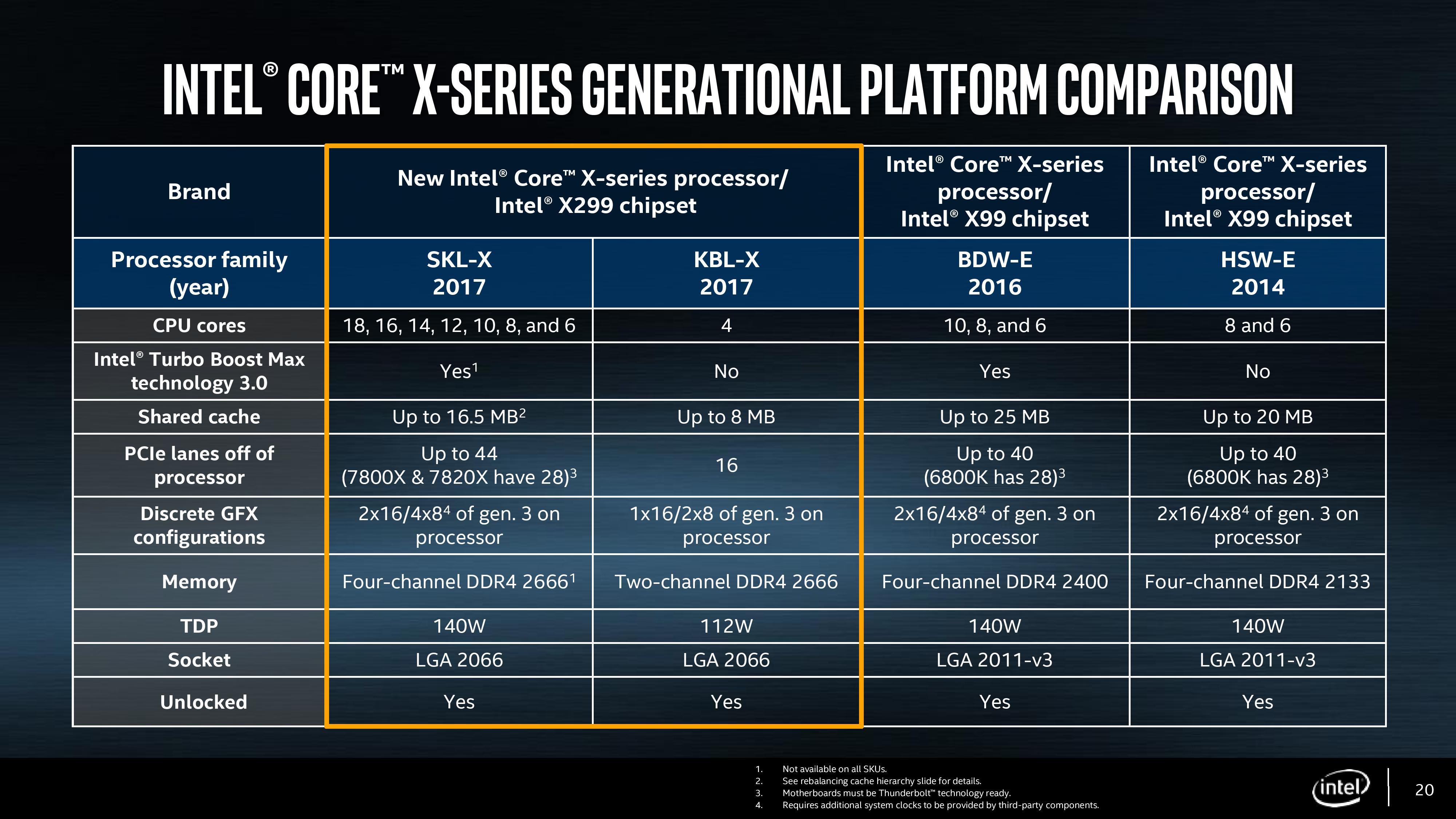
The Skylake-X family of processors for Basin Falls comes in two stages, based on the way the processors are developed. Normally HEDT processors are cut down versions of enterprise processors, usually through restricting certain functions, but the enterprise processors are typically derived from three different silicon layouts during manufacturing. Internally Intel call these three layouts the LCC (low core-count), HCC (high core-count) and XCC (extreme core-count), based on the maximum number of cores they support. Nominally Intel does not disclose which silicon layout they use for which processors, though it is usually straight forward to work them out as long as Intel has disclosed what the configurations of the LCC/HCC/XCC dies are. In this case, Intel has officially left everyone guessing, but the point here is that historically Intel only uses the LCC silicon from the enterprise line for its consumer desktop processors.
In previous generations, this meant either a 6, 8 or 10 core processor at the top of the stack for consumers, with lower core count models being provided by binning/salvaging imperfect CPUs. Each year we expected one of two things: the top-end SKU either gets more frequency, less power, or more cores, and as such the march of progress has been predictable. If you had asked us two months ago, we would have fully expected Skylake-X to top out with LCC silicon at 10 or 12 cores, depending on how Intel was planning the manufacturing part.
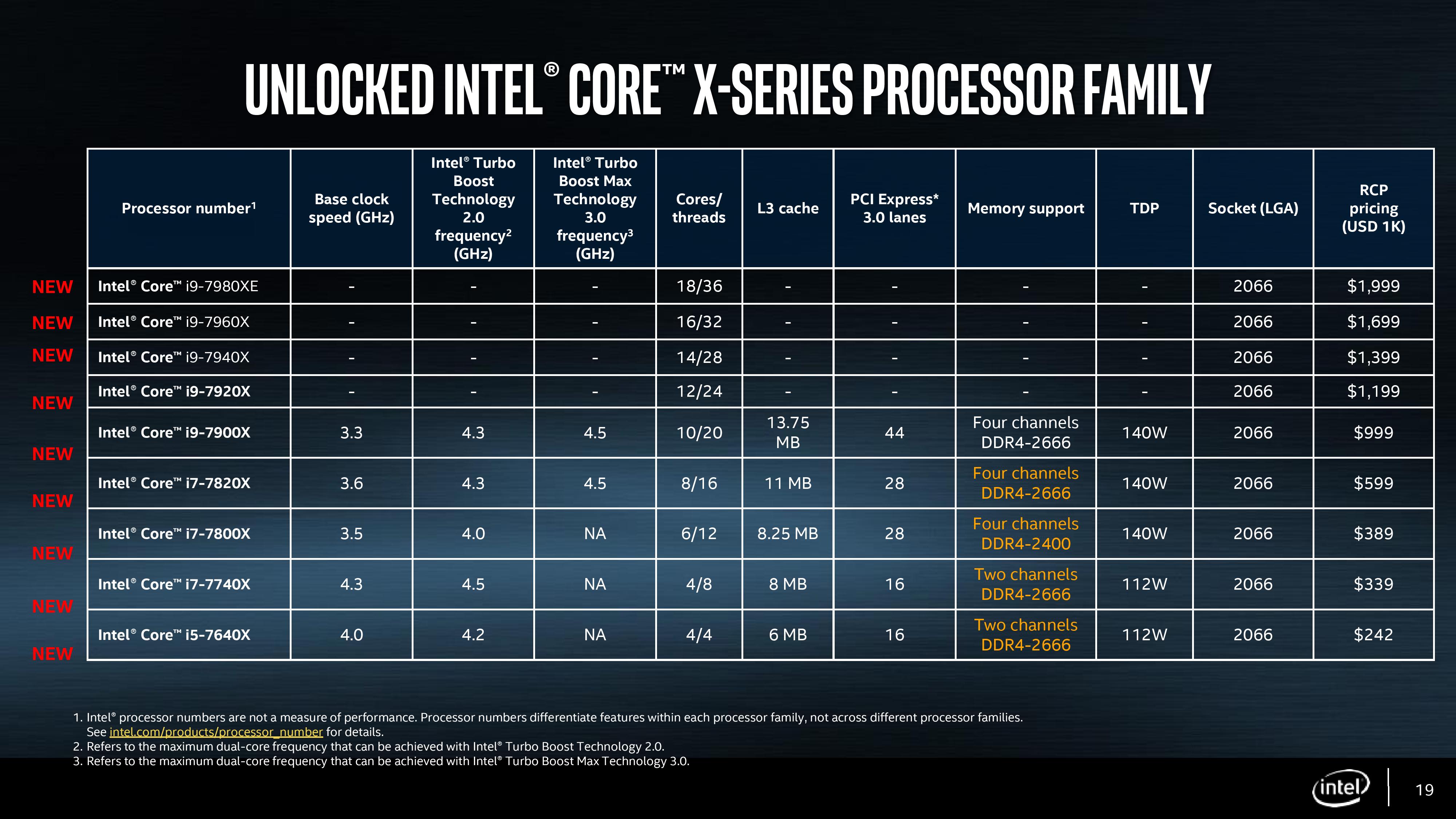
So the first element of Intel’s launch is the LCC processors, running up to 10 cores. We previously published that the LCC silicon was 12 cores, but we can now show it is 10 – more on that later. The three Skylake-X CPUs launching today are using LCC silicon with 6, 8 or 10 cores as the Core i7-7800X, Core i7-7820X and Core i9-7900X respectively. Intel is further separating these parts by adjusting the level of official supported DRAM frequency, as well as the PCIe lanes. We’ll go in a bit more detail further in the review.
The second element to the Skylake-X launch is the one that has somewhat surprised most of the industry: the launch will contain four processors based on the HCC silicon. Technically these processors will not be out until Q4 this year (one SKU coming out in August), and the fact that Intel did not have frequency numbers to share when announcing these parts shows that they are not finalized, calling into question when they were added to the roadmap (and if they were a direct response to AMD announcing a 16-core part for this summer). We’ve written a detailed analysis on this in our launch coverage, and we’ll cover some of the topics in this review. But Intel is set to launch 12, 14, 16 and 18-core consumer level processors later this year, with the top part running a tray price (when you buy 1k CPUs at a time) of $1999, so we expect the retail to be nearer $2099.
It should be noted that due to a number of factors, the Skylake-X cores and the communication pathways therein are built slightly differently to the consumer version of Skylake-S, which is something discussed and analyzed in this review.
The final element to the Basin Falls launch is Kaby Lake-X. This is also an aspect of the Basin Falls platform that deviates from the previous generations. Intel’s HEDT line has historically been one generation behind the mainstream consumer platform due to enterprise life cycles as well as the added difficulty of producing these larger chips. As a result, the enterprise and HEDT parts have never had the peak processing efficiency (IPC, instructions per clock) of the latest designs and have sat in the wings, waiting. By bringing the Kaby Lake microarchitecture to HEDT, this changes the scene, albeit slightly. Rather than bringing a new big core featuring the latest microarchitecture, Intel is repurposing the Kaby Lake-S mainstream consumer silicon, binning it to slightly more stringent requirements for frequency and power, disabling the integrated graphics, and then putting it in a package for the high-end desktop platform. There are still some significant limitations, such as having only 16 PCIe 3.0 lanes and dual channel memory, which might exclude it from the traditional designation of being a true HEDT processor, however Intel has stated that these parts fill a request from customers to have the latest microarchitecture on the HEDT platform. They also overclock quite well, which is worth noting.
The Kaby Lake-X parts will consist of a Core i7 and Core i5, both of which are quad core parts, with the i7 supporting hyperthreading. We have a parallel Kaby Lake-X review alongside our Skylake-X coverage, with some numbers from a stable 5 GHz overclock.


264 Comments
View All Comments
mat9v - Tuesday, June 20, 2017 - link
To play it safe, invest in the Core i9-7900X today.To play it safe and get a big GPU, save $400 and invest in the Core i7-7820X today.
Then the conclusion should have been - wait for fixed platform. I'm not even suggesting choosing Ryzen as it performs slower but encouraging buying flawed (for now) platform?
mat9v - Tuesday, June 20, 2017 - link
Please then correct tables on 1st page comparing Ryzen and 7820X and 7800X to state that Intel has 24 lines as they leave 24 for PCIEx slots and 4 is reserved for DMI 3.0If you strip Ryzen lines to only show those available for PCIEx do so for Intel too.
Ryan Smith - Wednesday, June 21, 2017 - link
The tables are correct. The i7 7800 series have 28 PCIe lanes from the CPU for general use, and another 4 DMI lanes for the chipset.PeterCordes - Tuesday, June 20, 2017 - link
Nice article, thanks for the details on the microarchitectural changes, especially to execution units and cache. This explains memory bandwidth vs. working-set size results I observed a couple months ago on Google Compute Engine's Skylake-Xeon VMs with ~55MB of L3: The L2-L3 transition was well beyond 256kB. I had assumed Intel wouldn't use a different L3 cache design for SKX vs. SKL, but large L2 doesn't make much sense with an inclusive L3 of 2 or 2.5MB per core.Anyway, some corrections for page3: The allocation queue (IDQ) is in Skylake-S is always 64 uops, with or without HT. For example, I looked at the `lsd.uops` performance counter in a loop with 97 uops on my i7-6700k. For 97 billion counts of uops_issued.any, I got exactly 0 counts of lsd.uops, with the system otherwise idle. (And I looked at cpu_clk_unhalted.one_thread_active to make sure it was really operating in non-HT mode the majority of the time it was executing.) Also, IIRC, Intel's optimization manual explicitly states that the IDQ is always 64 entries in Skylake.
The scheduler (aka RS or Reservation Station) is 97 unfused-domain uops in Skylake, up from 60 in Haswell. The 180int / 168fp numbers you give are the int / fp register-file sizes. They are sized more like the ROB (224 fused-domain uops, up from 192 in Haswell), not the scheduler, since like the ROB, they have to hold onto values until retirement, not just until execution. See also http://blog.stuffedcow.net/2013/05/measuring-rob-c... for when the PRF size vs. the ROB is the limit on the out-of-order window. See also http://www.realworldtech.com/haswell-cpu/6/ for a nice block diagram of the whole pipeline.
SKL-S DIVPS *latency* is 11 cycles, not 3. The *throughput* is one per 3 cycles for 128-bit vectors, or one per 5 cycles for 256b vectors, according to Agner Fog's table. I forget if I've tested that myself. So are you saying that SKL-SP has one per 5 cycle throughput for 128-bit vectors? What's the throughput for 256b and 512b vectors?
-----
It's really confusing the way you keep saying "AVX unit" or "AVX-512 unit" when I think you mean "512b FMA unit". It sounds like vector-integer, shuffle, and pretty much everything other than FMA will have true 512b execution units. If that's correct, then video codecs like x264/x265 should run the same on LCC vs. HCC silicon (other than differences in mesh interconnect latency), because they're integer-only, not using any vector-FP multiply/add/FMA.
-------
> This should allow programmers to separate control flow from data flow...
SIMD conditional operations without AVX512 are already done branchlessly (I think that's what you mean by separate from control-flow) by masking the input and/or output. e.g. to conditionally add some elements of a vector, AND the input with a vector of all-one or all-zero elements (as produced by CMPPS or PGMPEQD, for example). Adding all-zeros is a no-op (the additive identity).
Mask registers and support for doing it as part of another operation makes it much more efficient, potentially making it a win to vectorize things that otherwise wouldn't be. But it's not a new capability; you can do the same thing with boolean vectors and SSE/AVX VPBLENDVPS.
PeterCordes - Tuesday, June 20, 2017 - link
Speed Shift / Hardware P-State is not Windows-specific, but this article kind of reads as if it is.Your article doesn't mention any other OSes, so nothing it says is actually wrong: I'm sure it did require Intel's collaboration with MS to get support into Win10. The bullet-point in the image that says "Collaboration between Intel and Microsoft specifically for W10 + Skylake" may be going too far, though. That definitely implies that it only works on Win10, which is incorrect.
Linux has supported it for a while. "HWP enabled" in your kernel log means the kernel has handed off P-state selection to the hardware. (Since Linux is open-source, Intel contributed most of the code for this through the regular channels, like they do for lots of other drivers.)
dmesg | grep intel_pstate
[ 1.040265] intel_pstate: Intel P-state driver initializing
[ 1.040924] intel_pstate: HWP enabled
The hardware exposes a knob that controls the tradeoff between power and performance, called Energy Performance Preference or EPP. Len Brown@Intel's Linux patch notes give a pretty good description of it (and how it's different from a similar knob for controlling turbo usage in previous uarches), as well as describing how to use it from Linux. https://patchwork.kernel.org/patch/9723427/.
# CPU features related to HWP, on an i7-6700k running Linux 4.11 on bare metal
fgrep -m1 flags /proc/cpuinfo | grep -o 'hwp[_a-z]*'
hwp
hwp_notify
hwp_act_window
hwp_epp
I find the simplest way to see what speed your cores are running is to just `grep MHz /proc/cpuinfo`. (It does accurately reflect the current situation; Linux finds out what the hardware is actually doing).
IDK about OS X support, but I assume Apple has got it sorted out by now, almost 2 years after SKL launch.
Arbie - Wednesday, June 21, 2017 - link
There are folks for whom every last compute cycle really matters to their job. They have to buy the technical best. If that's Intel, so be it.For those dealing more with 'want' than 'need', a lot of this debate misses an important fact. The only reason Intel is suddenly vomiting cores, defecating feature sizes, and pre-announcing more lakes than Wisonsin is... AMD. Despite its chronic financial weakness that company has, incredibly, come from waaaay behind and given us real competition again. In this ultra-high stakes investment game, can they do that twice? Maybe not. And Intel has shown us what to expect if they have no competitor. In this limited-supplier market it's not just about who has the hottest product - it's also about whom we should reward with our money, and about keeping vital players in the game.
I suggest - if you can, buy AMD. They have earned our support and it's in our best interests to do so. I've always gone with Intel but have lately come to see this bigger picture. It motivated me to buy an 1800X and I will also buy Vega.
Rabnor - Wednesday, June 21, 2017 - link
To play it safe and get a big GPU, save $400 and invest in the Core i7-7820X today.You have to spend that $400+ on a good motherboard & aio cooler.
Are you sold by Intel, anandtech?
Synviks - Thursday, June 22, 2017 - link
For some extra comparison: running Cinebench R15 on my 14c 2.7ghz Haswell Xeon, with turbo to 3ghz on all cores, my score is 2010.Pretty impressive performance gain if they can shave off 4 cores and end up with higher performance.
Pri - Thursday, June 22, 2017 - link
On the first page you wrote this:Similarly, the 6-core Core i7-7820X at $599 goes up against the 8-core $499 Ryzen 7 1800X.
The Core i7 7820X was mistakenly written as a 6-core processor when it is in-fact an 8-core processor.
Kind Regards.
Gigabytes - Thursday, June 22, 2017 - link
Okay, here is what I learned from this article. Gaming performance sucks and you will be able to cook a pizza inside your case. Did I miss anything?Oh, one thing missing.
Play it SMART and wait to see the Ripper in action before buy your new Intel toaster oven.