Samsung and TSMC Roadmaps: 8 and 6 nm Added, Looking at 22ULP and 12FFC
by Anton Shilov on May 5, 2017 9:30 AM EST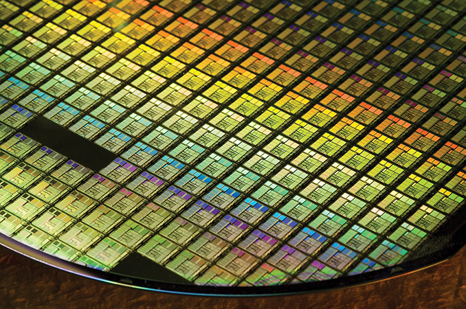
Samsung and TSMC made several important announcements about the present and future of their semiconductor manufacturing technologies in March. Samsung revealed that it had shipped over 70 thousand wafers processed using its first-generation 10 nm FinFET fabrication process (10LPE) and also announced major additions to its upcoming manufacturing technology roadmap. In particular, the company plans to introduce three processes it has not talked about thus far. TSMC said that it is about to start mass production of ICs (integrated circuits) using its first-gen 10 nm technology and also announced several new processes that will be launched in the coming years, including its first 7 nm EUV process due in 2019.
10 nm: Samsung Is Shipping
Update 5/12: Samsung informed us that its press release from October, 2016, compares characteristics of the 10LPE manufacturing technology with those of the 14LPE, not 14LPP. The text and table have been updated accordingly.
Samsung said it had started to make SoCs using its 10LPE fabrication technology last October, which is something we already knew. This manufacturing process allowed the company to make its chips 30% smaller compared to ICs made using its 14LPE process as well as reducing power consumption by 40% (at the same frequency and complexity) or increase their frequency by 27% (at the same power and complexity). So far, Samsung has processed over 70 thousand wafers using its 10LPE technology, which can give an idea about Samsung’s 10 nm production capacities (considering that the whole 10 nm production cycle is greater than the 90 days we saw with previous-gen FinFET processes). At the same time, keep in mind that Samsung does not have many 10 nm designs to manufacture right now: we know only of the company’s own Exynos 9 Octa 8895 as well as Qualcomm’s Snapdragon 835 seen in the Samsung Galaxy S8.
| Advertised PPA Improvements of New Process Technologies Data announced by companies during conference calls, press briefings and in press releases |
||||||||
| GF | Samsung | |||||||
| 7nm DUV vs 14LPP |
14LPP vs 28LPP |
10LPE vs 14LPE |
10LPE vs 14LPP |
10LPP vs 10LPE |
10LPU vs 10LPE |
|||
| Power | >60% | 60% | 40% | 30% | ~15% | ? | ||
| Performance | >30% | 40% | 27% | >10% | ~10% | ? | ||
| Area Reduction | >50% | 50% | 30% | 30% | none | ? | ||
In addition to its production milestone, Samsung also confirmed plans to start mass production of chips using its second-generation 10 nm manufacturing process called 10LPP (10 nm low-power plus) by the end of 2017 as well as its third-generation 10 nm technology called 10LPU by the end of 2018. Samsung said last year that the 10LPP is going to enable a ~10% performance increase (at the same power and at the same complexity) versus the 10LPE, but we know absolutely nothing about the 10LPU. It is logical to assume that the 10LPU will bring certain PPA-related (performance, power, area) improvements, but it is not clear how Samsung plans to achieve them and which one of the three will be the focus for improvements. As it appears, just like Intel, Samsung has ended up with three generations of 14 nm fabrication processes and is going to end up with three generations of 10 nm manufacturing technologies. It is noteworthy that Samsung itself does not use its 14LPC (low-power compact) for its leading edge SoCs, which may suggest that the 10LPU is also not aimed at this segment of the market. In fact, it is highly likely that the 10LPU will target ultra-small and ultra-low-power ICs for various emerging devices, but Samsung yet has to confirm that.
10nm: TSMC Is Steady
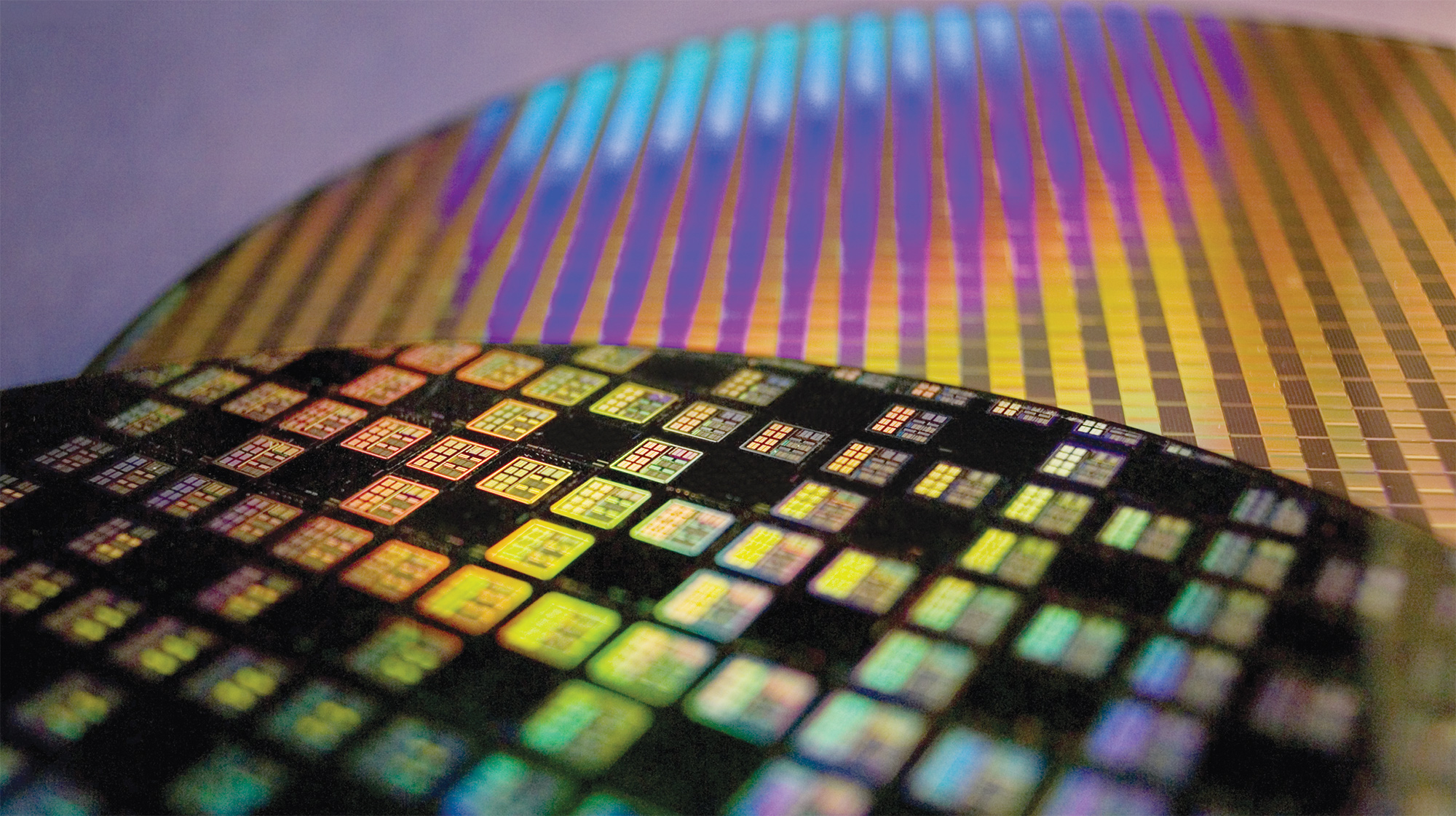
As for TSMC, its 10 nm process technology (CLN10FF) is now qualified for production at the company’s GigaFabs 12 and 15, where high-volume ramp is expected to start in H2 2017. Production capacity of these two fabs is hundreds of thousands wafer starts per quarter and TSMC plans to ship 400 thousand wafers processed using its 10 nm manufacturing tech this year. Considering the long production cycles for FinFET-based technologies, it is about time for TSMC to start ramping up 10 nm so to be able to supply enough chips to its main customer in time. Apple is expected to launch its new iPhone products in September or October and needs to get SoCs couple of months before the launch.
| Advertised PPA Improvements of New Process Technologies Data announced by companies during conference calls, press briefings and in press releases |
|||||||
| TSMC | |||||||
| 16FF+ vs 28HPM |
16FF+ vs 20SOC |
10FF vs 16FF+ |
7FF vs 16FF+ |
7FF vs 10FF |
|||
| Power | 70% | 60% | 40% | 60% | <40% | ||
| Performance | 65% | 40% | 20% | 30% | ? | ||
| Area Reduction | ~50% | none | >50% | 70% | >37% | ||
PPA advantages of TSMC’s CLN10FF over its CLN16FF+ (second-gen 16 nm) have been discussed already and they are significant for developers of mobile SoCs (but not that significant for makers of other ICs): a ~50% higher transistor density, a 20% performance improvement at the same power and complexity or a 40% lower power consumption at the same frequency and complexity. Unlike Samsung, TSMC does not seem to plan multiple generations of 10 nm and will go straight to 7 nm next year. 7nm is currently very popular among chip designers, indicating a future major milestone. However, in addition to the CLN7FF, the company will also offer several other manufacturing technologies for ultra-small and ultra-low-power applications.


89 Comments
View All Comments
vladx - Friday, May 5, 2017 - link
Yep I'm skeptical about a software development revolution, I think focusing on better computer architectures has a much better outlook.melgross - Saturday, May 6, 2017 - link
Well, there's the question of whether we can get a revolutionary computer architecture these days. It not easy. So we're still looking at cisc vs risc. Maybe we need to go more risc and less cisc. Pretty much everything is some combo of the two.ABR - Sunday, May 7, 2017 - link
No revolution, but technology has been and will continue advancing here for a long time. Higher-level languages and object-oriented programming making larger projects possible. Evolution in UI frameworks and asynchronous programming (cutting edge in mobile frameworks). Hardware virtualization, network definition migrating to software, and environment encapsulation (e.g., Docker), simplifying resource management. Frameworks like OpenGL, EX, Metal bridging the gap between graphics and graphics hardware. Libraries like Caffe and TensorFlow doing the same for neural networks and learning software.Also engineering tools and techniques. Distributed version control systems for source code management. Suites like dpkg or maven for handling dependencies. Team and process practices like the family of Agile techniques.
The sophistication and sheer amount and ubiquity of software applications in our lives today depends just as much on all of these things as on faster, lower power hardware.
boeush - Saturday, May 6, 2017 - link
Once we reach the absolute quantum limits of 2d scaling, we will be looking at alternative materials (graphene, nanotubes, diamond, III-IV chemistry, etc) for better power and frequency scaling. At the same time, 3D stacking of 2D layers by the dozens, then hundreds, then thousands. At the same time, advanced heat dissipation tech (graphene/nanotubes/diamond could serve double duty there), as well as (at least for non-portable devices) refrigeration not just for overclocking but for normal operation. Maybe even look into superconducting chips/interconnects using high-Tc materials, immersed in liquid Nitrogen... There's also research into molecular computing. And, of course, you can always trade off generality against special purpose accelerator ASICs that can provide many-orders-of-magnitude speedup vs conventional processors on same node in specific tasks: and the more compact the node, the more of these various narrow-use circuits you can affordably cram onto a single chip...melgross - Saturday, May 6, 2017 - link
Sure, there are a lot of technologies out there. But most are just impractical, or just too expensive, and complex. We've has liquid cooling for some time, but do most people really want that? What about notebooks? Can't really be done.Other technologies have been considered for a couple of decades but as so expensive that envelope mainframe CPUs can't use them.
Most of these technologies can be used for every high end use, because of expense, effectiveness, and even power draw. But that's just for the top 0.1% of computing. What about the rest of us?
ironargonaut - Monday, May 8, 2017 - link
You mean like when they said that the physics of light would prevent any geometries less then 193nm? Sorry, but the "wall" that was going to end CPU density increases has been broken so many times, that I won't believe it till I see it. Of course just because all those predictions where wrong doesn't mean yours is. Cheers.Gich - Friday, May 5, 2017 - link
Some time ago I dig up this:"14/16nm":
Intel ~13.4nm - from Broadwell to Coffee Lake, Atom x5/x7
Samsung/GFo ~16.6nm - AMD Zen and Rx400/500, nVidia 1050, SD 620/820, Exynos 7/8, Apple A9
TSMC ~18.3nm - nVidia 1060+, Apple A9/10
"10nm":
Intel ~9.5nm - Cannonlake
TSMC ~11.3nm - Helio X30, Kirin 970, Apple A10X
Samsung ~12.0nm - SD835, Exynos 9
Gich - Friday, May 5, 2017 - link
"7nm":Intel ~6.7nm
TSMC/GF ~8.2nm
Samsung ~8.4nm
smalM - Monday, May 8, 2017 - link
TSMC ~18.3nm - that's 16FF which was never used for mass production but is always used by Intel for comparison...helvete - Thursday, July 20, 2017 - link
Intel paper, intel's point of view.