Intel’s 140GB Optane 3D XPoint PCIe SSD Spotted at IDF
by Ian Cutress on August 26, 2016 12:01 PM EST- Posted in
- SSDs
- Intel
- Enterprise
- Enterprise SSDs
- 3D XPoint
- IDF_2016
- Optane
As part of this year’s Intel’s Developer Forum, we had half expected some more insights into the new series of 3D XPoint products that would be hitting the market, either in terms of narrower time frames or more insights into the technology. Last year was the outing of some information, including the ‘Optane’ brand name for the storage version. Unfortunately, new information was thin on the ground and Intel seemed reluctant to speak any further about the technology that what had already been said.
What we do know is that 3D XPoint based products will come in storage flavors first, with DRAM extension parts to follow in the future. This ultimately comes from the fact that storage is easier to implement and enable than DRAM, and the characteristics for storage are not as tight as those for DRAM in terms of break-neck speed, latency or read/write cycles.
For IDF, Optane was ultimately relegated to a side presentation at the same time as other important talks were going on, and we were treated to discussions about ‘software defined cache hierarchy’ whereby a system with an Optane drive can define the memory space as ‘DRAM + Optane’. This means a system with 256GB of DRAM and a 768GB Optane drive can essentially act like a system with ‘1TB’ of DRAM space to fill with a database. The abstraction layer in the software/hypervisor is aimed at brokering the actual interface between DRAM and Optane, but it should be transparent to software. This would enable some database applications to move from ‘partial DRAM and SSD scratch space’ into a full ‘DRAM’ environment, making it easier for programming. Of course, the performance compared to an all-DRAM database is lower, but the point of this is to move databases out of the SSD/HDD environment by making the DRAM space larger.
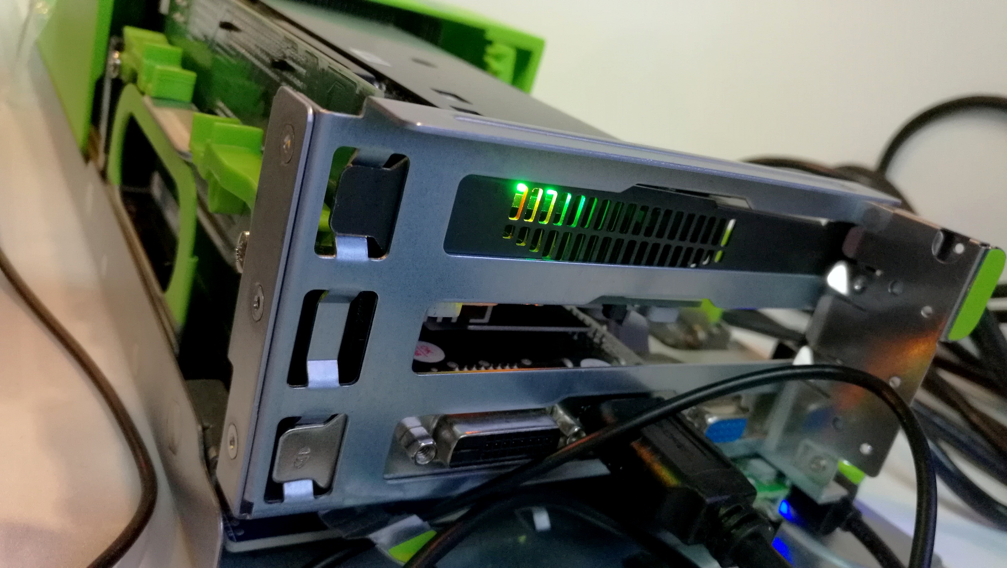
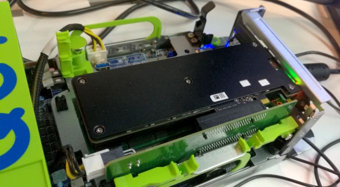
Aside from the talk, there were actually some Optane drives on the show floor, or at least what we were told were Optane. These were PCIe x4 cards with a backplate and a large heatsink, and despite my many requests neither demonstrator would actually take the card out to show what the heatsink looked like. Quite apart from which, neither drive was actually being used - one demonstration was showing a pre-recorded video of a rendering result using Optane, and the other was running a slideshow with results of Optane on RocksDB.
I was told in both cases that these were 140 GB drives, and even though nothing was running I was able to feel the heatsinks – they were fairly warm to the touch, at least 40C if I were to narrow down a number. One of the demonstrators was able to confirm that Intel has now moved from an FPGA-based controller down to their own ASIC, however it was still in the development phase.
Click through for high resolution
One demo system was showing results from a previous presentation given earlier in the lifespan of Optane: rendering billions of water particles in a scene where most of the scene data was being shuffled from storage to memory and vice versa. In this case, compared to Intel’s enterprise PCIe SSDs, the rendering reduced down from 22hr to ~9hr.
It's worth noting that we can see some BGA pads on the image above. The pads seem to be in an H shape, and there are several present, indicating that these should be the 3D XPoint ICs. Some of the pads are empty, suggesting that this prototype should be a model that offers a larger size. Given the fact that one of the benefits of 3D XPoint is density, we're hoping to see a multi-terabyte version at some point in the distant future.
The other demo system was a Quanta / Quanta Cloud Technology system node, featuring two Xeon E5 v4 processors and a pair of PCIe slots on a riser card – the Optane drive was put into one of these slots. Again, it was pretty impossible to see more of the drive aside from its backplate, but the onscreen presentation of RocksDB was fairly interesting, especially as it mentioned optimizing the software for both the hardware and Facebook.
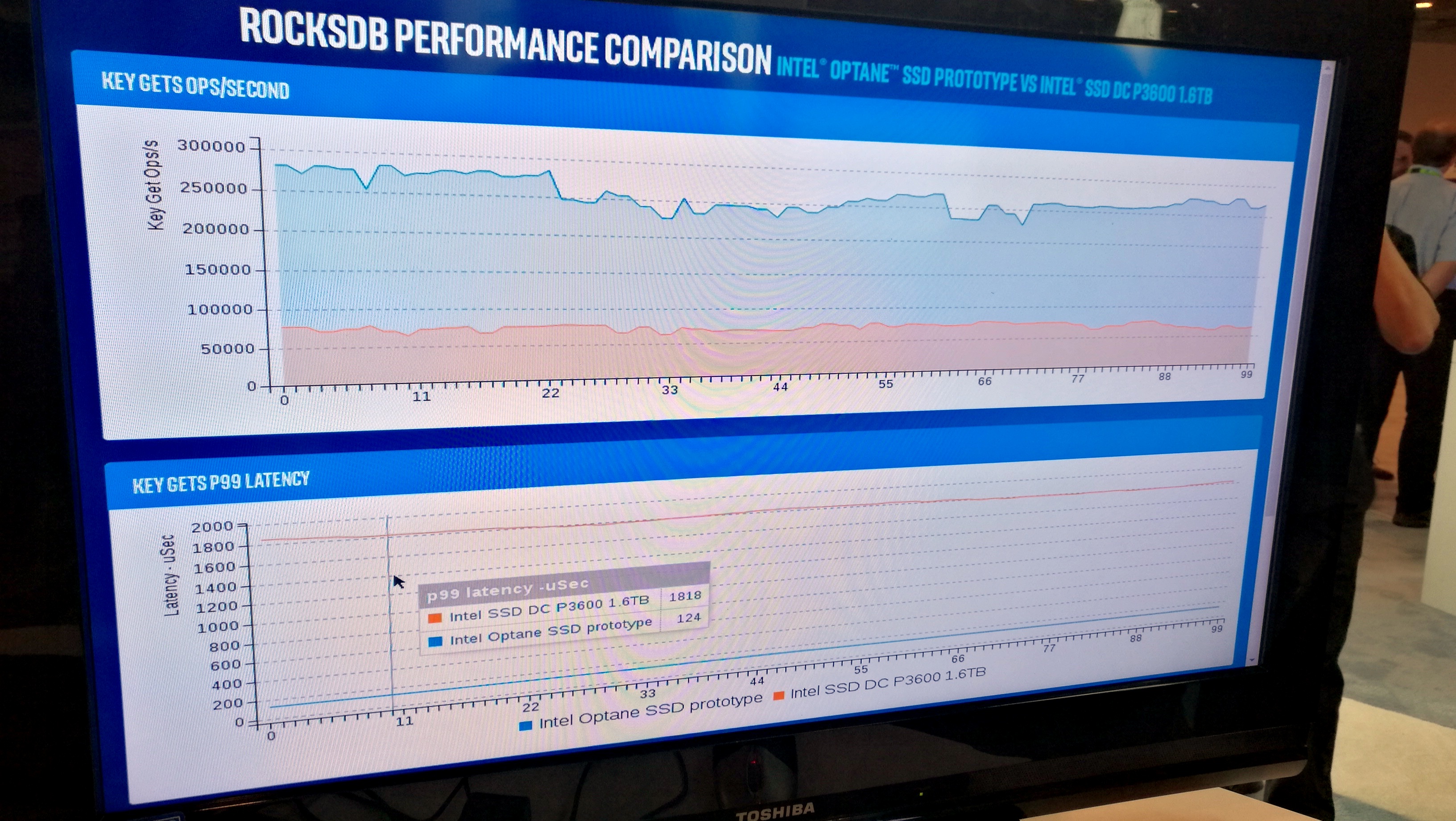
RocksDB is a high-performance key/store database designed for fast embedded storage, used by Facebook, LinkedIn and Yahoo, but the fact that Facebook was directly involved in some testing indicates that at some level the interest in 3D XPoint will brush the big seven cloud computing providers before it hits retail. In the slides on screen, the data showed a 10x reduction in latency as well as a 3x improvement in database GETs. There was a graph plotted showing results over time (not live data), with the latency metrics being pretty impressive. It’s worth noting that there were no results shown for storing key/value data pairs.
Despite these demonstrations on the show floor, we’re still crying out for more information about 3D XPoint, how it exactly work (we have a good idea but would like confirmation), Optane (price, time to market) as well as the generation of DRAM products for enterprise that will follow. With Intel being comparatively low key about this during IDF is a little concerning, and I’m expecting to see/hear more about it during Supercomputing16 in mid-November. For anyone waiting on an Optane drive for consumer, it feels like it won’t be out as soon as you think, especially if the big seven cloud providers are wanting to buy every wafer from the production line for the first few quarters.
More images in the gallery below.


66 Comments
View All Comments
Omoronovo - Friday, August 26, 2016 - link
Unless you have some Intel insider knowledge, I don't think we can really be sure yet exactly how far Xpoint will scale, or even if it eventually turns into some other form of technology (like ReRAM, as you said). Intel certainly hasn't gone into that much depth yet, and even this teaser was just a side event at IDF, so clearly Intel doesn't want to let us all know yet.Honestly, I'm just really excited to see how this technology evolves, and to find out more about it. I'm guessing the low-key nature of this means Intel won't be wanting to give an hard, in-depth looks at the technology for quite a while yet.
jjj - Friday, August 26, 2016 - link
I've mentioned a redrand in my first comment so don't insist on that. Yes they could keep the name even if it's substantially different solution.The difference between XPoint and a"proper"solution is like the difference between 2D NAND with more than 1 layer and 3D NAND.
With 3D XPoint they just add layers and that's why costs aren't scaling great. AT in their first article on Xpoint i think mentions that Intel/Micron hope that EUV arrives soon and helps them scale.
3D NAND is designed so you can process multiple layers in 1 step. Fewer steps = lower costs and shorter cycles. Shorter cycles helps costs further, as the cost.
Here how they make their 3D NAND http://www.chipworks.com/about-chipworks/overview/...
They deposit the layers, they etch and then you got a few more steps where many layers are processed in 1. That's where the bulk of the cost saving are supposed to come and this is what makes it a "true"3D.
XPoint is not as smart as that, they just add layer after layer and that's why it's not ideal from a cost perspective.
Went and found the AT article i've mentioned , the first section is relevant "The Technology: How Does 3D XPoint Work?"http://www.anandtech.com/show/9470/intel-and-micro... t
saratoga4 - Friday, August 26, 2016 - link
>3D NAND is designed so you can process multiple layers in 1 step. Fewer steps = lower costs and shorter cycles. Shorter cycles helps costs further, as the cost.Are you sure about that? Micron I think was supposed to have a slightly more efficient process than Samsung, but as far as I know scaling is still O(N) masks where N is the number of layers in the memory array.
jjj - Friday, August 26, 2016 - link
Isn't this the entire point of 3D NAND? Otherwise they would just add layers of 2D NAND. Guess BeSang is trying to just add high density layers, we'll see how it goes.Anyway,Micron and Intel are somewhat constrained on the vertical,on the horizontal and hard to say how easy it might be to add bits per cell.
A " proper" solution would have more freedom in at least 2 of those.
XPoint would have served it's purpose without the delays. Owning the market for a few years and scaling a little bit to stay alive for a while even after the competition responds.
With the delays,we might see some volumes next year and real volumes in 2018 so its future is rather murky.
saratoga4 - Friday, August 26, 2016 - link
>Isn't this the entire point of 3D NAND?The point of 3D NAND is to allow stacking of NAND cells vertically so that you can improve density without having to pay for multi-patterning. It doesn't necessarily reduce the number of steps (actually I think it requires a lot more) as compared to planar, but it does result in lower costs per bit since you don't need multipatterning.
jjj - Friday, August 26, 2016 - link
On WD's thingy the author completely misses the point but you have this quote " Western Digital indicated that it would use some of the things it has learnt while developing its BiCS 3D NAND to produce its ReRAM chips. " http://www.anandtech.com/show/10562/western-digita...The presentation was called "Creating Storage Class Memory: Learning from 3D NAND" so it's very clear that their entire point was this ,how to make it scale properly.
floobit - Friday, August 26, 2016 - link
Their latency numbers seem a bit different than your analysis of the P3700 in http://www.anandtech.com/show/8104/intel-ssd-dc-p3... Can you explain? ~20@QD1, then 200@QD32, and 800 us @QD128 in your article, and they have 1800 us by "thread".Krysto - Friday, August 26, 2016 - link
We already know the price - it's 4x higher than NVMe drives per GB, which themselves are about 3x higher than mainstream SATA 3 SSDs. So it should be at least 10-12x more expensive than a 140GB SATA 3 SSD. If it's meant for "enterprise customers", then you can easily double that price yet again.So my guess is at the very least $1,000 for 140GB drive. Potentially on the higher-end of that $1,000, too.
Omoronovo - Friday, August 26, 2016 - link
There are very few directly-comparable AHCI and NVME devices, but the ones I looked at directly (The samsung SM951 drives) have almost zero difference in price. In fact, on average, the NVME 256/512GB version of that drive is actually about 5% cheaper, possibly just due to supply/demand.Fundamentally, there is no reason why the signalling interface should have any bearing on the cost of the device; I think you are probably comparing m.2 drives with 2.5" drives, which is not a fair cost comparison since m.2 drives generally need denser (and hence costlier) NAND modules to reach the same capacities whist fitting into smaller physical space.
Assuming these storage devices from Intel ship as standard PCI-E devices (either directly or via m.2 form factor), then hopefully the 4x figure is the only one that will matter. There is no way one of these will use AHCI as the signalling protocol since the cpu overhead would be enormous at anything approaching the iops figures quoted in the article.
TheinsanegamerN - Monday, August 29, 2016 - link
A 512GB samsung 950 pro is over $300. $350 ATM. a SM951 is $339.A 512GB sata III SSD is only $150 for a high end model. A 1TB is only $239 for a mushkin reactor. A samsung m.2 sata drive at 500 GB is only $169.
NVME certainly commands a price premium.