Western Digital to Use 3D ReRAM as Storage Class Memory for Special-Purpose SSDs
by Anton Shilov on August 12, 2016 8:00 AM EST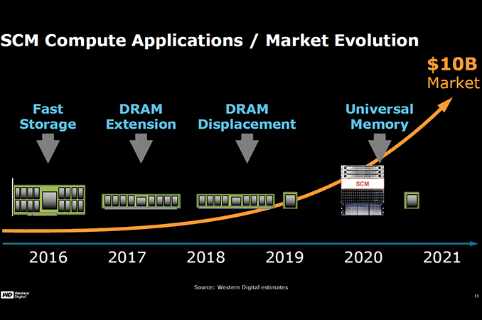
At the Flash Memory Summit this week, Western Digital announced that it intends to use 3D Resistive RAM (ReRAM) as storage class memory (SCM) for its future special-purpose ultra-fast SSDs. The company did not reveal any actual timelines for appropriate products, nor their specifications. However, what is important is the fact that Western Digital decided to use SanDisk’s long-discussed ReRAM along with 3D manufacturing tech to build the aforementioned special-purpose SSDs.
The amount of data that the world produces totals several zettabytes per year, which creates two challenges for the high-tech industry: one is to store the vast amounts of data more or less cost-efficiently, another is to process this data efficiently from power consumption point of view. Modern SSDs and HDDs can store plenty of information (10 to 15 TB for top-of-the-range models) and modern CPUs can process a lot of data due to increasing number of cores. However, delivering the right data to those cores poses further challenges: if the necessary data is located on an HDD/SSD, fetching them from there takes a lot of time on computer timescales (e.g., 100,000 – 10,000,000 ns) and consumes a lot of energy. Meanwhile, increasing the amount of DRAM per server is not always feasible from economic point of view.

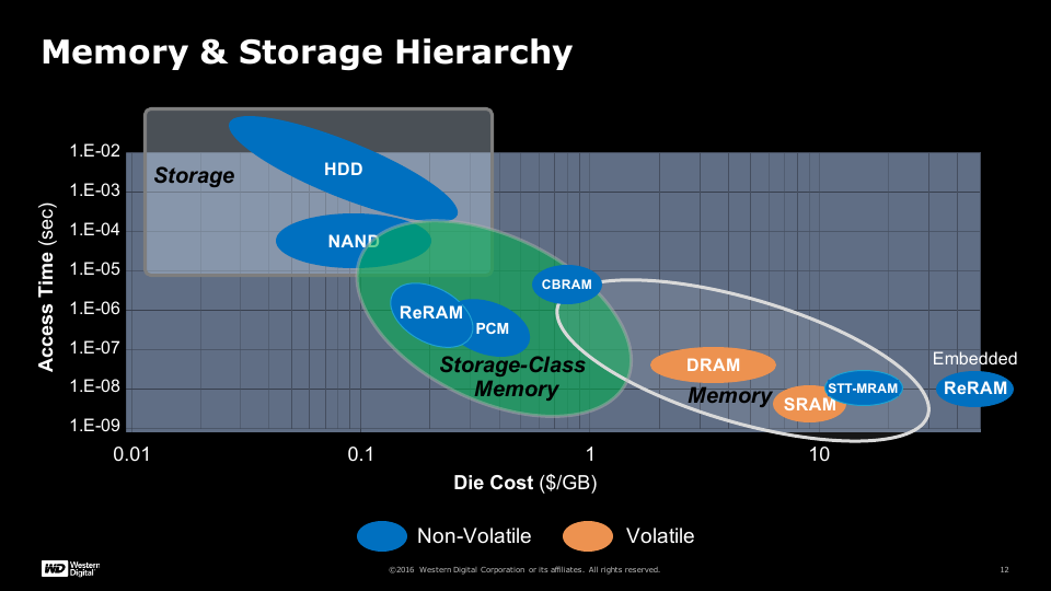
To address the challenge, the industry came up with idea of non-volatile SCM, which would sit between DRAM and storage devices and deliver much greater performance, endurance and lower latency (e.g., 250 – 5,000 ns) than NAND while costing a lot less than DRAM in terms of per-GB prices. Historically, different companies demonstrated various types of memory, which could be used as SCM (originally, this class of devices was classified as a replacement tech for NAND flash), including conductive-bridging RAM (CBRAM), phase-change memory (PCM), magnetoresistive RAM (MRAM), resistive RAM (ReRAM) and some others. All of these technologies have their own peculiarities like performance and costs (and none of them could beat NAND in terms of per-GB cost), but SanDisk has been working for years on bringing ReRAM to the market.
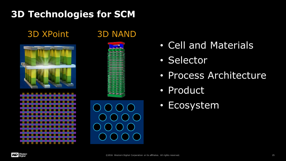
Fundamentally, ReRAM (also sometimes called RRAM) works by changing the resistance across a dielectric material by electrical current (which is why 3D XPoint is considered as a proprietary implementation of ReRAM). The resistance can be measured and considered as “0” or “1”. On paper, the technology enables higher performance and endurance when compared to NAND flash, but finding the right materials and architecture for ReRAM has taken engineers many years.
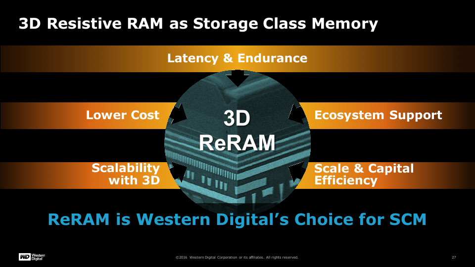
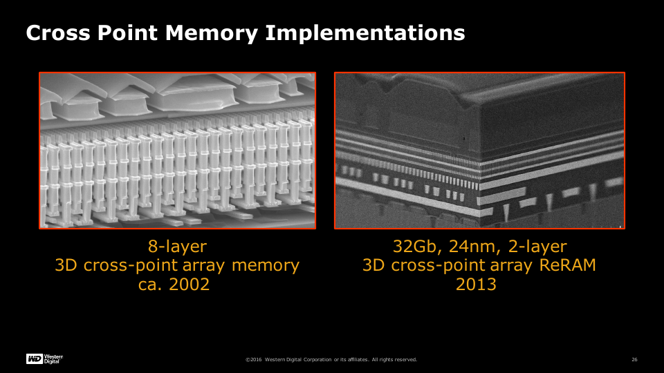
Without making any significant announcements this week, Western Digital indicated that it would use some of the things it has learnt while developing its BiCS 3D NAND to produce its ReRAM chips. The company claims that its ReRAM will feature a multi-layer cross-point implementation, something it originally revealed a while ago.
Perhaps, the most important announcement regarding the 3D ReRAM by Western Digital is the claim about scale and capital efficiency of the new memory. Essentially, this could mean that the company plans to use its manufacturing capacities as well as its infrastructure (testing, packaging, etc.) in Yokkaichi, Japan, to make 3D ReRAM. Remember that SCM is at this point more expensive than NAND, hence, it makes sense to continue using the current fabs and equipment to build both types of non-volatile memory so ensure that the SCM part of the business remains profitable. IMFT does the same thing with its SCM: it uses its fab in Lehi, Utah, to produce 3D XPoint memory, but does not reveal specifics about the process technology (just like Western Digital). Of course, Western Digital could re-use some of the fundamental technologies, materials and process architecture both for ReRAM and NAND, but the company does not any particular details on the matter just now.
Quite naturally, WD’s 3D ReRAM will scale in terms of per-IC densities with the increase of the number of layers, though, we do not know how many layers will initial 3D ReRAM ICs from Western Digital incorporate. However, the company seems to be very optimistic about scaling of its SCM and believes that over time it will close the gap in terms of per-GB cost with BiCS NAND and will thus widen the gap with DRAM, which will make it more economically feasible.

Finally, the manufacturer said that its 3D ReRAM is already supported by the ecosystem, which means that the first SSDs based on the technology will probably use industry-standard interfaces (e.g. NVDIMM), which is not surprising. Perhaps, it also means that Western Digital is also already working with software developers to ensure that applications can take advantage of SCM in general, but we cannot confirm this at this time.
To sum up, Western Digital has finished development of ReRAM, which SanDisk has been discussing for several years now. The company plans to release actual products based on ReRAM in the foreseeable future (12 – 24 months from now, call it a guess) and to use the same fab and equipment to build ReRAM and NAND ICs. Western Digital’s ReRAM has a roadmap for the future. What remains to be seen is what is going to happen to the joint development of SCM announced by SanDisk and HP in October, 2015.


Source: Western Digital


38 Comments
View All Comments
jjj - Friday, August 12, 2016 - link
"Western Digital decided to use SanDisk’s long-discussed ReRAM along with 3D manufacturing tech to build the aforementioned special-purpose SSDs"Sandisk's ReRAM has always been 3D, the way you phrase it suggests that it's a new idea.
Capital intensity and scaling is not about using the same clean room, that's not where the big costs are.
The comparison with what Micron and Intel are doing is way off. Yes ofc they are using the same clean rooms but XPoint is not using much of the same tools and they have to spend a lot, it's very capital intensive and it doesn't scale all that well.
The main point that you should have been able to figure out just from the title of the presentation is that there is a big cost difference between just adding layers (like XPoint) and something that is designed for 3D (like 3D NAND). Fewer process steps, shorter cycle, less fab area and so on is what makes the cost difference.
That's the main point, adding layers by just repeating the same steps won't result in costs scaling well. A clever design where you process multiple layers in 1 step leads to costs scaling much better.
Maybe this helps understand how 3D NAND is not just adding layers http://www.chipworks.com/about-chipworks/overview/...
rahvin - Friday, August 12, 2016 - link
This is why Intel/Micron aren't providing details about Xpoint. HP is supposedly got one in the works based on memsistors along with the FeRAM that's out there as well. They won't tip their hand until product is shipping because of this.Penti - Friday, August 12, 2016 - link
So this is Sandisk/Toshiba's ReRAM effort? With a WD-branding? I.e. they will ship WD drives/end user products with ReRAM "soon" I guess. But I guess OEM customers (with previous relationship with Sandisk) still get their stuff...dealcorn - Friday, August 12, 2016 - link
I interpret this WD news as a failed homage to Edwin Land's observation "Someone is going to make your product obsolete. Make sure it's you." The market will ultimately decide who wins, but I see the deck as strongly and intentionally stacked in Intel's favor. While XPoint's virtues are viable through a variety of current interfaces, the full benefits of XPoint require a faster interface such as the DIMM interface Intel promises with Kaby Lake. Intel will ship XPoint using any interface it can, but once Kaby Lake arrives, I expect the faster DIMM interface to dominate sales to the data center which is where most SCM will be sold. If you pay a substantial premium for performance, it is dumb to leave performance on the table by using an inferior interface. I doubt Intel's firmware behind the Kaby Lake DIMM socket will support competitive products that are not XPoint. If you exclude Data Center demand for SCM, the remaining demand that is willing to pay premium prices, such as high end gaming, is table scraps that may not be adequate to support an economic ramp.Often, in tech, he who ramps first and fastest wins. Even the technical superiority of Beta could not overcome the faster ramp of VHS. WD's release spec's make it sound like a wannabe XPoint except the it is not yet in production and WD can not yet show a sample or tout performance advantages which may not be known at this time. Intel is already in production and ramps while we sleep. The concept that WD can leverage Wannabe technology applied to table scraps market demand to create a competitive product is definitely possible if the technology is vastly superior enough. I do not get that vibe from what WD is saying today.
Ultimately, after a successful ramp reduces costs significantly, XPoint escapes the confines of the Data Center and goes everywhere. However, Data Center dominance is the most likely and perhaps only path to a successful ramp.
name99 - Saturday, August 13, 2016 - link
Wrong wrong wrong. ("However, Data Center dominance is the most likely and perhaps only path to a successful ramp.")The other possible route is that Apple uses SCM on the iPhone 2018 (or whatever) as a way to yet again bump up IO speed and responsiveness. Then, after a few years, the rest of the phone market follows.
If I were WD/SanDisk this is the path I'd try to follow (i.e. be willing to make whatever changes and meet the price points Apple want some). But WD have not been an especially forward looking company in the past (witness their lack of interest in SSDs and hybrids for so long) so I would not be optimistic that they're smart enough to do this.
vladx - Saturday, August 13, 2016 - link
With 3D XPoint offering ~1000x lower latency than NAND I don't know how this can compete with that. Too late. Sandisk/WDiwod - Monday, August 15, 2016 - link
So basically this is WD / Sandisk version of Optane. The interesting bit is ( assume the scale and graphs are correct ) we will reach ReRAM 10x cheaper /GB then DRAM at around 2019. If we assume DRAM dont get any cheaper, we could get a $40 80 ReRAM Drive in 2019.But where are the bottlenecks? We have PCI-E SSD Drives that offer 2x IOPS and 4x Bandwidth compared to best of SATA SSD, and they offer negligible UX difference in 80-90% use cases.
So may be it is a matter of Software that needs some fundamental changes?
LukaP - Monday, August 15, 2016 - link
The bottlenecks arent so much in the consumer space (the UX you refer to) but more in the HPC and server space, where many applications are very IO bound (eg databases) and there, even the fastest of SSDs still bottleneck the CPU