NVIDIA Announces Quadro Pascal Family: Quadro P6000 & P5000
by Ryan Smith on July 25, 2016 4:45 PM EST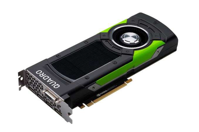
If there was one word to describe the launch of NVIDIA’s Pascal generation products, it’s “expedient.” On the consumer side of the business the company has launched 3 different GeForce cards and announced a fourth (Titan X), while on the HPC side the company has already launched their Tesla P100 accelerator, with the PCIe version due next quarter. With the company moving so quickly it was only a matter of time until a Quadro update was announced, and now today at SIGGRAPH 2016 the company is doing just that.
Being announced today are the two Quadro models that will fill out the high-end of the Quadro family, the P6000 and P5000. As hinted at by the name, these are based on NVIDIA’s latest Pascal generation GPUs., marking the introduction of Pascal to the Quadro family. And like NVIDIA’s consumer counterparts, these new cards should offer significant performance and feature upgrades over their Maxwell 2 based predecessors.
| NVIDIA Quadro Specification Comparison | ||||||
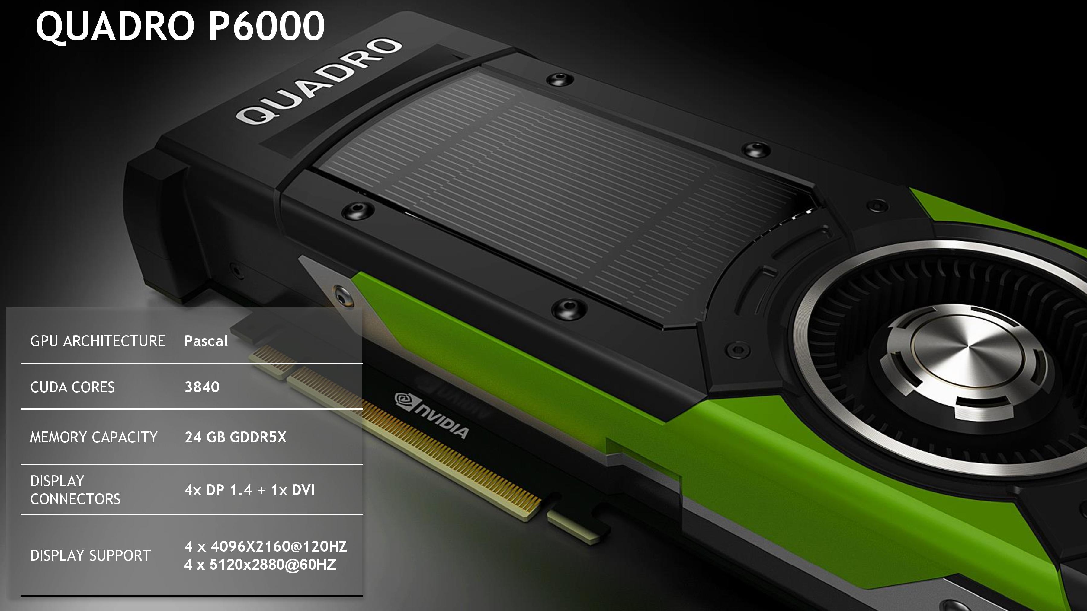
| P6000 | P5000 | M6000 | M5000 | |||
| CUDA Cores | 3840 | 2560 | 3072 | 2048 | ||
| Texture Units | 240? | 160 | 192 | 128 | ||
| ROPs | 96? | 64 | 96 | 64 | ||
| Core Clock | ? | ? | N/A | N/A | ||
| Boost Clock | ~1560MHz | ~1730MHz | ~1140MHz | ~1050MHz | ||
| Memory Clock | 9Gbps GDDR5X | 9Gbps GDDR5X | 6.6Gbps GDDR5 | 6.6Gbps GDDR5 | ||
| Memory Bus Width | 384-bit | 256-bit | 384-bit | 258-bit | ||
| VRAM | 24GB | 16GB | 24GB | 8GB | ||
| FP64 | 1/32 FP32 | 1/32 FP32 | 1/32 FP32 | 1/32 FP32 | ||
| TDP | 250W | 180W | 250W | 150W | ||
| GPU | GP102 | GP104 | GM200 | GM204 | ||
| Architecture | Pascal | Pascal | Maxwell 2 | Maxwell 2 | ||
| Manufacturing Process | TSMC 16nm | TSMC 16nm | TSMC 28nm | TSMC 28nm | ||
| Launch Date | October 2016 | October 2016 | 03/22/2016 | 08/11/2015 | ||
| Launch Price (MSRP) | TBD | TBD | $5000 | $2000 | ||
We will start, as always, at the top, with the Quadro P6000. As NVIDIA’s impending flagship Quadro card, this is based on the just-announced GP102 GPU. The direct successor to the GM200 used in the Quadro M6000, the GP102 mixes a larger number of SMs/CUDA cores and higher clockspeeds to significantly boost performance.
Paired with P6000 is 24GB of GDDR5X memory, running at a conservative 9Gbps, for a total memory bandwidth of 432GB/sec. This is the same amount of memory as in the 24GB M6000 refresh launched this spring, so there’s no capacity boost at the top of NVIDIA’s lineup. But for customers who didn’t jump on the 24GB – which is likely a lot of them, including most 12GB M6000 owners – then this is a doubling (or more) of memory capacity compared to past Quadro cards. At this time the largest capacity GDDR5X memory chips we know of (8Gb), so this is as large of a capacity that P6000 can be built with at this time. Meanwhile this is so far the first and only Pascal card with GDDR5X to support ECC, with NVIDIA implementing an optional soft-ECC method for the DRAM only, just as was the case on M6000.
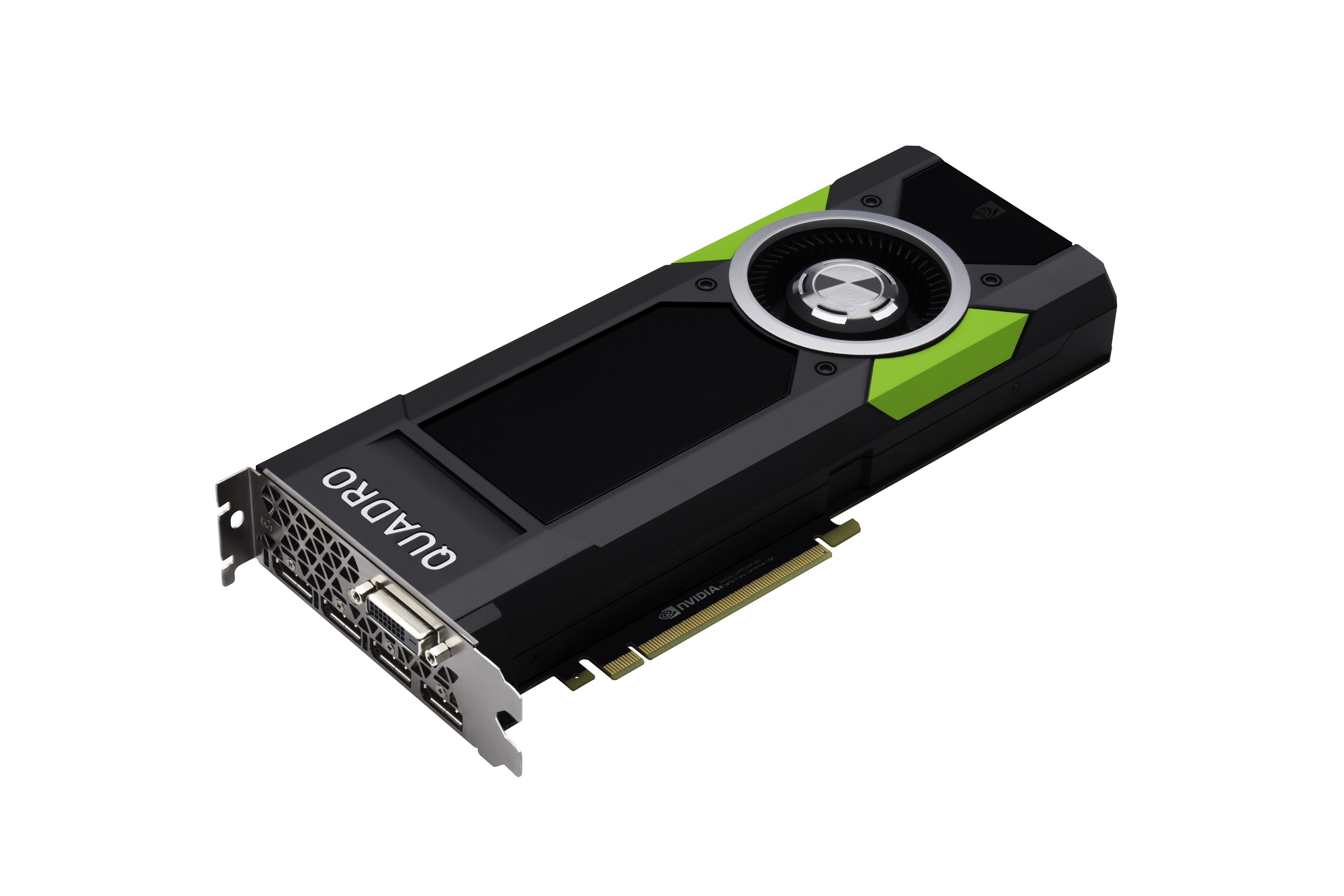
NVIDIA has also sent over pictures of the card design, and confirmed that the card ships with the Quadro 6000-series standard TDP of 250W. Utilizing the same basic metal shroud and blower design as the M6000 cards, the P6000 should be suitable as drop-in replacement for older M6000 cards. Do note however that like M6000, external power is pulled via a single 8-pin power connector, so technically this card is out of spec (not that this was a problem for M6000).
Unfortunately in their zeal to get this announcement out in time for SIGGRAPH - a frequent venue for Quadro announcements – we don’t have specific performance numbers available. NVIDIA has not locked down the GPU clockspeeds, and as a result we don’t just how P6000s clockspeeds and total throughput will compare to M6000’s. It goes without saying that it should be higher, but how much higher remains to be seen.
For overall expected performance, NVIDIA has published that the P6000 is rated for 12 TFLOPs FP32. Given that it's a fully enabled GP102 we're looking at, this works out to a clockspeed of around 1560MHz. On paper this gives P6000 around 71% more shading performance and 37% more ROP throughput than the older Maxwell 2 M6000. This also puts the P6000 around 9% ahead of the recently announced NVIDIA Titan X.
On a quick technical note, as this announcement comes just 4 days after NVIDIA announced the GP102 GPU used on this card, this Quadro announcement does confirm a few more things about GP102. Quadro P6000 ships with 3840 CUDA cores (30 SMs), confirming our earlier suspicions that GP102 was a (or at least) 30 SM part. Meanwhile this also confirms that GP102 can be outfit with 24GB of GDDR5X. Finally, NVIDIA has confirmed that there’s no high-speed FP64 support on GP102, which is why we’re looking at a 1/32 rate for even the top Quadro card.
M5000
Moving on, let’s talk about Quadro M5000. Based on NVIDIA’s GP104 GPU, this is the smaller, cheaper, lower power sibling to the P6000. This is a fully enabled part with all 2560 CUDA cores (20 SMs) active, so the performance gains versus M5000 should be similar to what we saw with the consumer GeForce GTX 1080. Clockspeeds are also comparable, so we're looking at sizable boost in shading/compute/texture performance of 2.06x, and ROP throughput has increased by 65%. Of the two cards, M5000 is going to the bigger upgrade versus its direct predecessor.
Meanwhile on the memory front, P5000 is equipped with 16GB of GDDR5X memory. This is attached to GP104’s 256-bit memory bus, and like P6000 is clocked at 9Gbps. P5000’s predecessor, M5000, maxed out at just 8GB of memory, so along with a 36% increase in memory bandwidth, this doubles the amount of memory available for a Quadro 5000 tier card.
Looking at the card design itself, to no surprise it strongly resembles the M5000, with its plastic blower dressed up in Quadro livery. The card’s TDP stands at 180W, which is a slight increase over M5000, but shouldn’t too significantly impact the drop-in replacement nature of the design.
Pascal Features & Availability
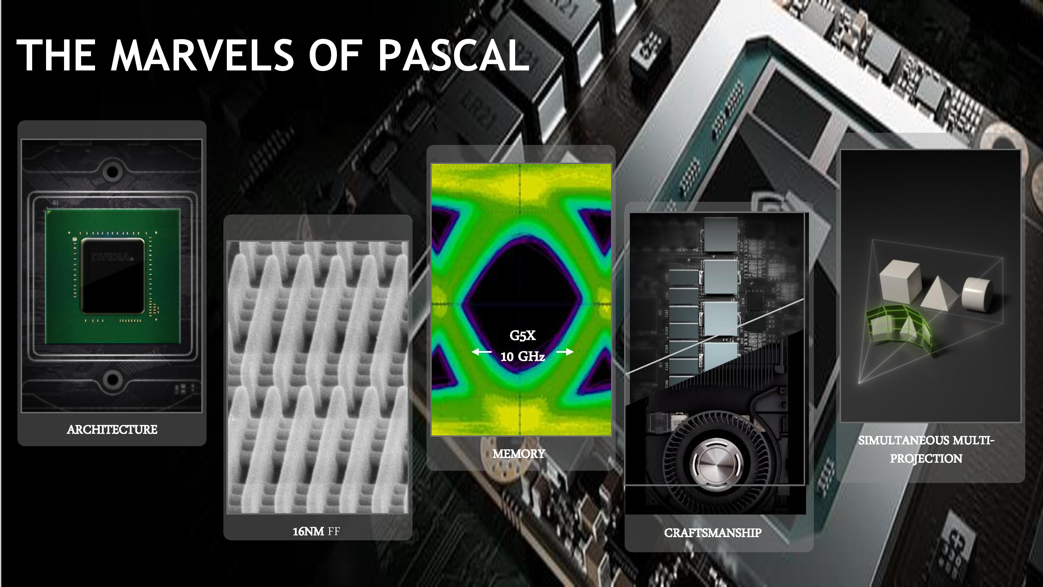
Along with the significant performance increase afforded by the Pascal architecture and TSMC’s 16nm FinFET manufacturing process, the other big news here is of course the functionality that comes to the Quadro P-series courtesy of Pascal. While for our regular readers there’s nothing new we haven’t seen already with GeForce, Pascal’s new functionality will apply a bit differently to the Quadro lineup.
Perhaps the biggest change here is Pascal’s new display controller. With both the P6000 and P5000 shipping with 4 DisplayPorts, the DisplayPort 1.4 capable controller means that both cards can now support higher resolutions and refresh rates. Whereas the M-series maxed out at 4 4K@60Hz monitors, the P-series can now handle 4 monitors running 5K@60Hz, 4 4K monitors running at 120Hz, or even 8K monitors with additional limitations. Do note however that the per-card monitor limit is still 4 displays, as this is as many displays as Pascal can support.
Speaking of multiple displays, alongside the Quadro card announcements NVIDIA is also announcing a new Quadro Sync card, the aptly named Quadro Sync 2. The multi-adapter/multi-display timing synchronization card is being updated to support the Pascal cards, and will support a larger number of adapters as well. The new Sync 2 will support 8 cards in sync, as opposed to 4 on the original Sync card. Coupled with the 4 display per card capability of Pascal, and this means synchronized video walls and other systems can now be built out to 32 displays.
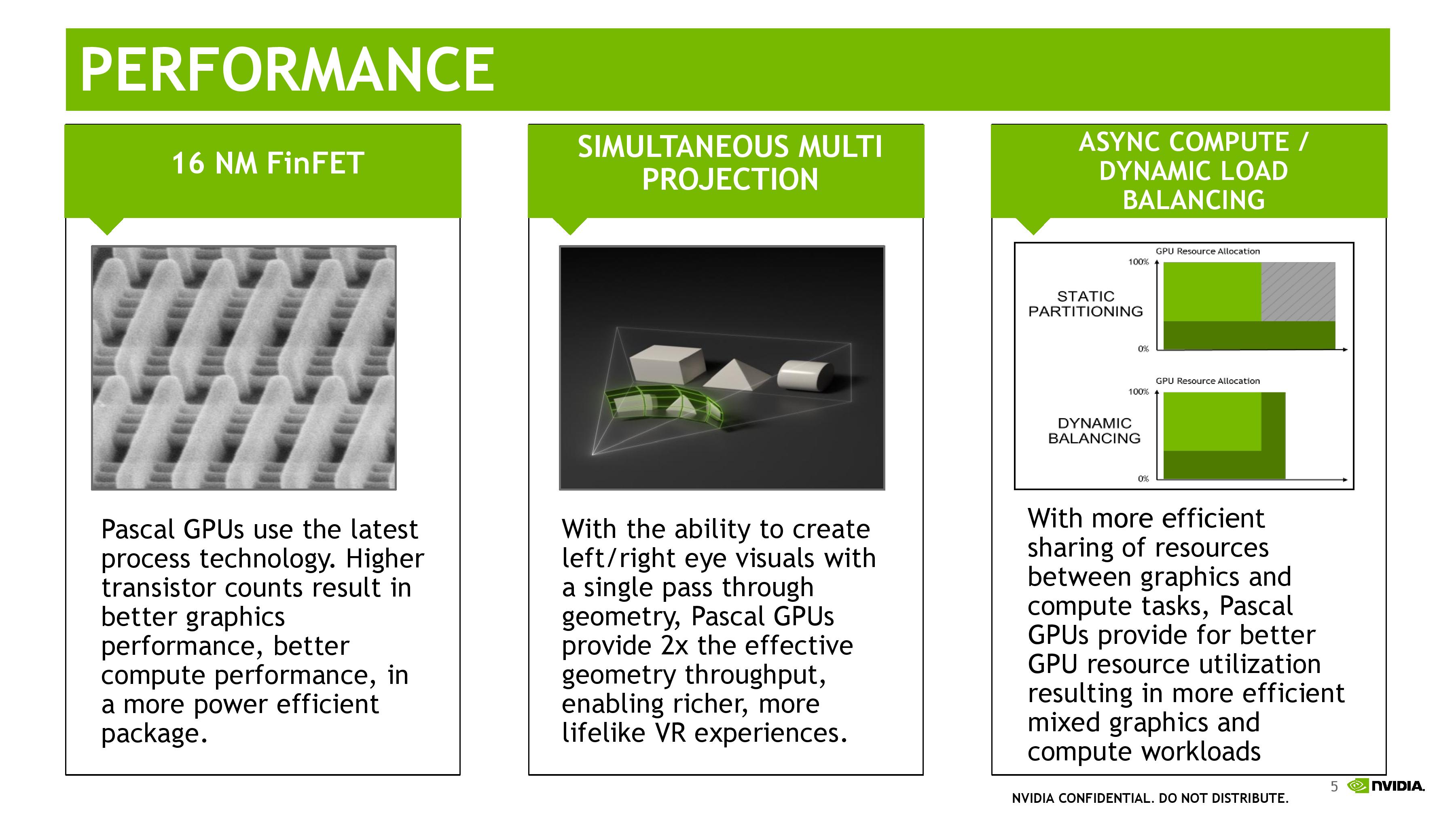
NVIDIA will also be heavily promoting Simultaneous Multi-Projection (SMP), the company’s multi-viewport technology. Like the consumer cards, VR is a big driver here, with NVIDIA looking reach out to VR developers. NVIDIA is also pitching this at VR CAVE systems, as they can see similar benefits from SMP’s geometry reprojection.
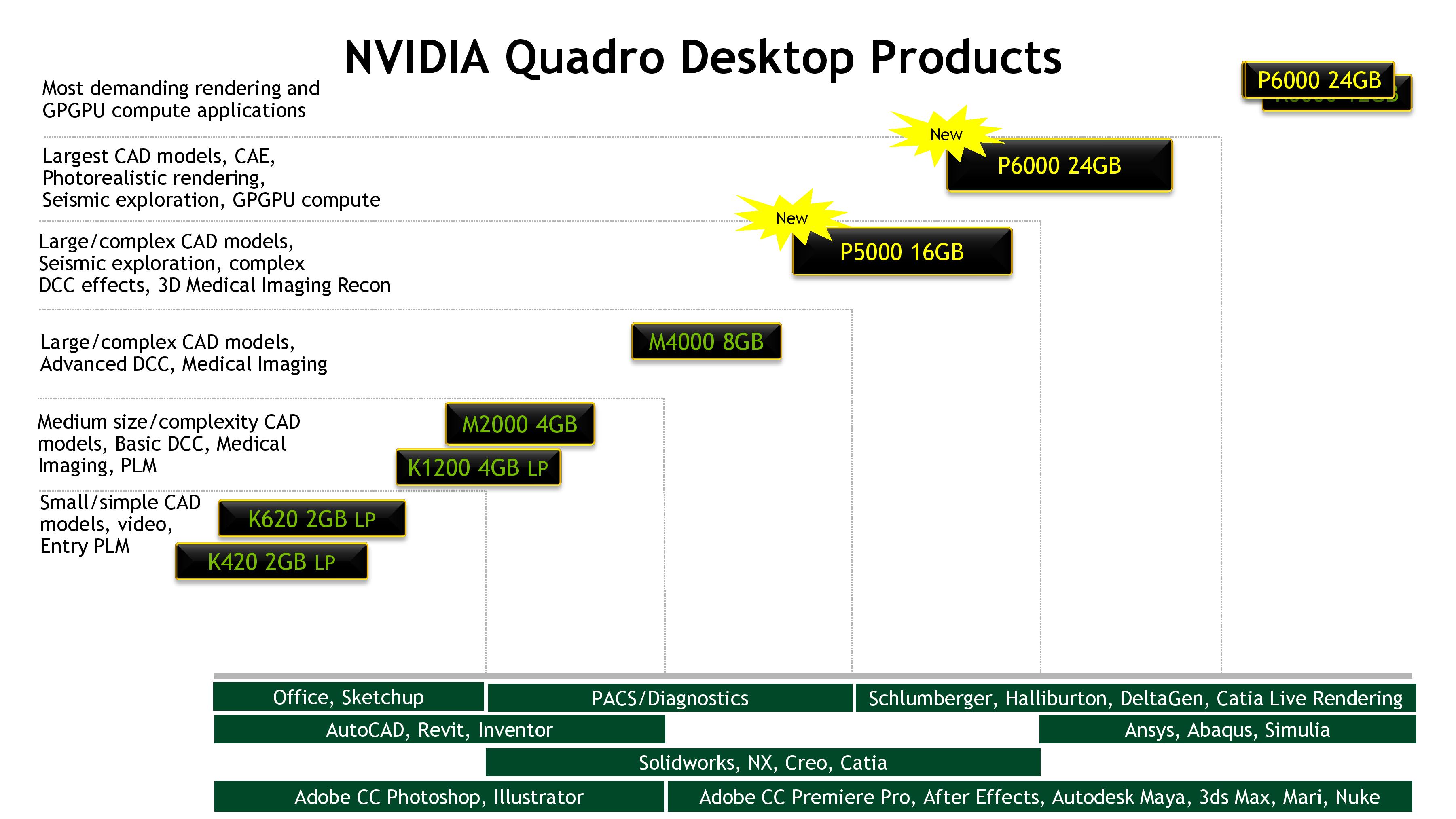
Taking a look at the overall Quadro lineup, the P6000 and P5000 will at least for the time being be sitting alongside the existing M4000 and lower cards. Within the Quadro lineup these cards are meant for the most demanding workloads– massive memory sets and complex rendering/compute tasks – and they will be priced accordingly. Specific pricing has not been announced, but NVIDIA tells us to expect them to be priced similarly to the last generation cards. This would work out to $5000+ for Quadro P6000, and $2000+ for Quadro P5000 at launch.
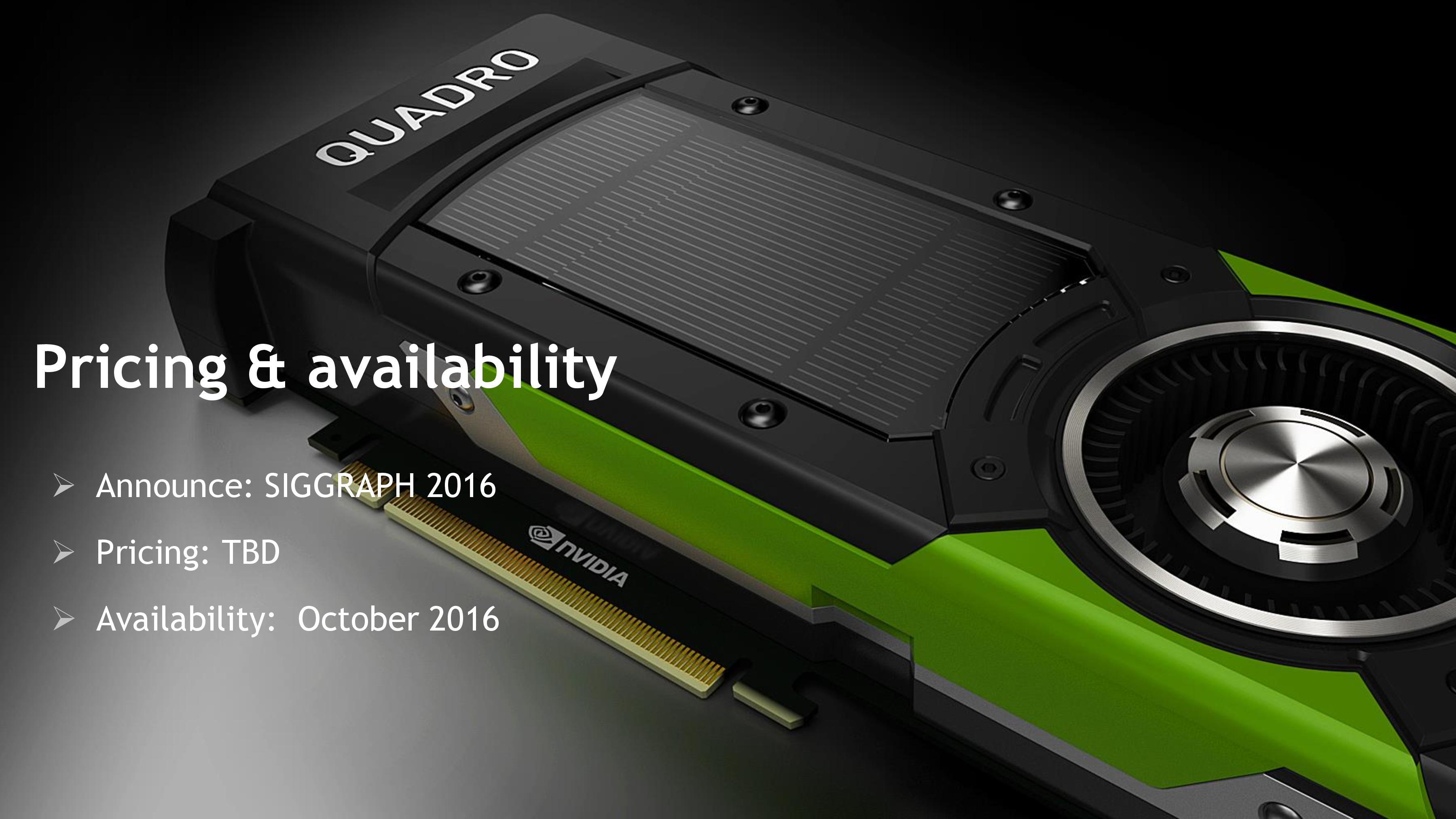
Finally, as we mentioned before NVIDIA was announcing these cards early, before the final clockspeeds have been locked down. This means that while the cards are being announced today, they won’t launch for another two months; NVIDIA expects them to be available in early October. It’s not unusual for Quadro cards to be announced ahead of time, though as SIGGRAPH is also a popular venue for AMD pro card announcements, the earlier than usual announcement may have been for multiple reasons.
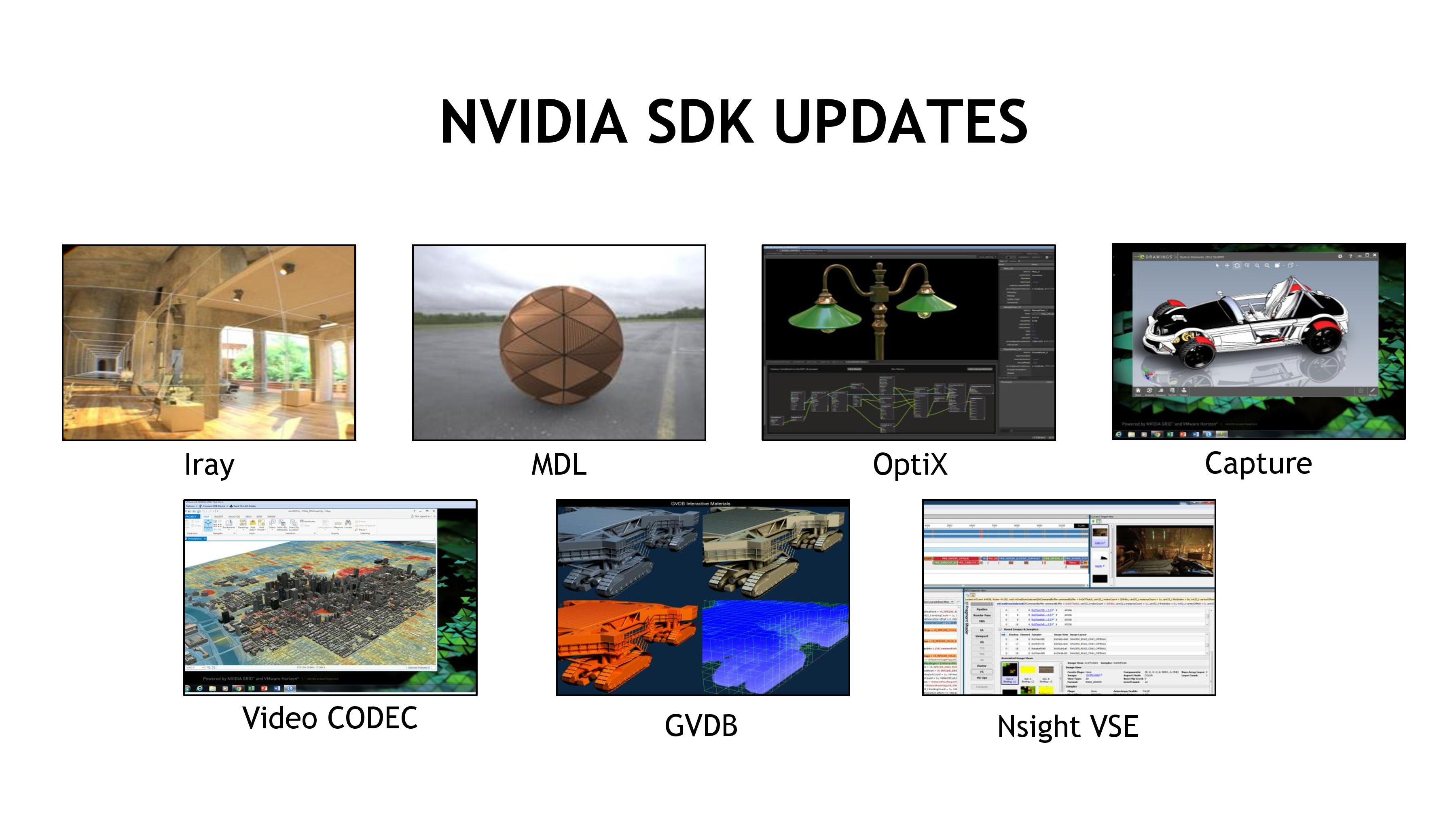
Ecosystem Announcements: New SDKs, Iray VR, & OptiX 4
Along with the announcement of the Quadro P-series, NVIDIA is also using SIGGRAPH to announce updates to various software and ecosystem initiatives within the company. Overall a number of the company’s SDKs are receiving an update in some form, ranging from rendering to video encode and capture, the latter taking advantage of Pascal’s 8K encode/decode capabilities.
Of particular note here, NVIDIA’s Iray physically based render plugin for 3D modeling applications is getting a significant update. As with other parts of their ecosystem, NVIDIA is doubling down on VR here as well. The next update to Iray will include support for generating panoramic VR lightfields – think high detail fixed position 3D panoramas – which can then be displayed on other devices. NVIDIA has been showing off an early version of this technology at GTC 2016 and other events, where it was used to show off renders of the company’s under-construction headquarters.
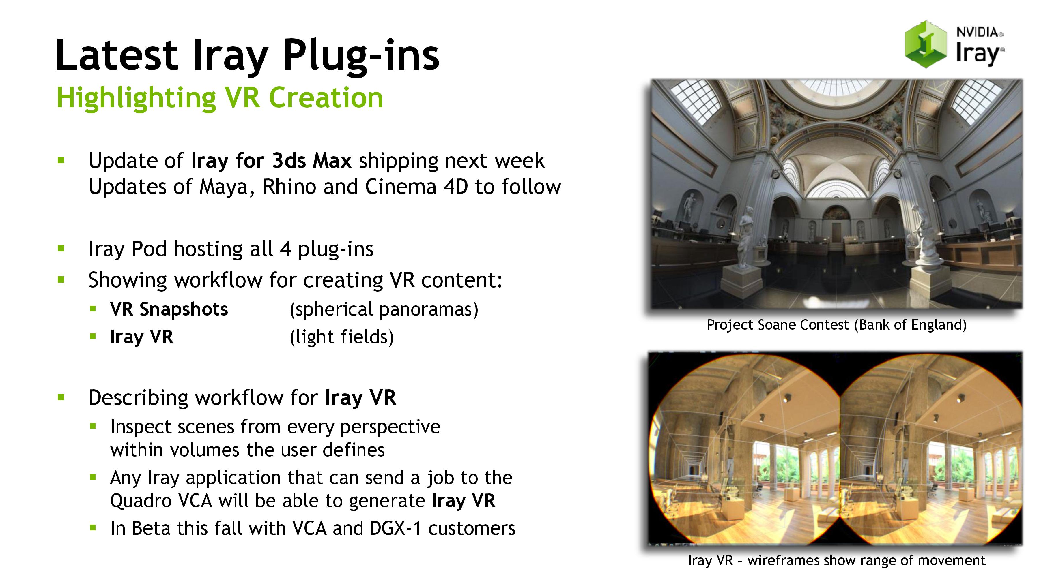
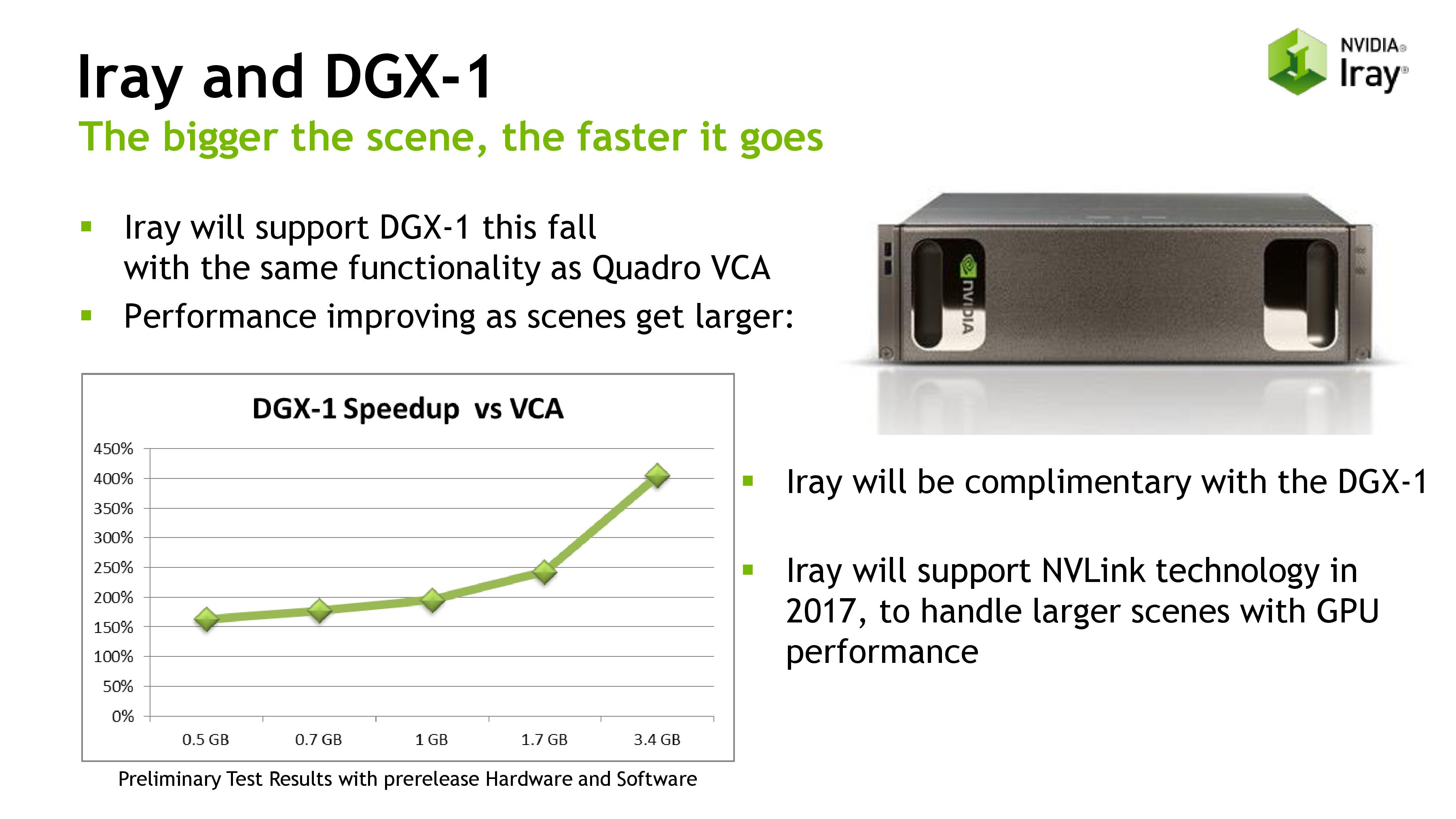
The Iray update will also be part of a larger focus on integrating the company’s software with their DGX-1 server, which incorporates 8 Tesla P100 accelerators. Iray will be coming to DGX-1 this fall, supporting the same features that are already available in multi-GPU setups with the older Quadro VCA. Longer term, in 2017, the company will be adding NVLink support for better multi-GPU scaling.
NVIDIA’s OptiX ray tracing engine is the other product that’s getting a DGX-1 update. OptiX 4.0, which is being released this week, adds support for the DGX-1, including NVLink support. It is interesting to note though that the company is only supporting clusters of 4 GPUs, despite the fact that DXG-1 has 8 GPUs (the other 4 GPUs form a second cluster). This may mean that OptiX needs direct GPU links to perform best – as in an 8-way configuration, some GPUs are 2 hops away – or it may just be that OptiX naturally doesn’t scale well beyond 4 GPUs.

Finally, NVIDIA is also announcing a change to how mental ray support is handled for Maya. Previous, integrating the ray tracer with Maya was handled by Autodesk, but NVIDIA is currently in the process of taking that over. The goal of doing so is to allow mental ray to be updated and have features added at the more brisk pace that NVIDIA tends to work at. The new plugin is currently scheduled to ship in September, and as one of their first actions, NVIDIA will be integrating a new global illumination engine, GI-Next.


40 Comments
View All Comments
extide - Tuesday, July 26, 2016 - link
It doesn't, it has the same amount, the die got smaller because they ripped out all the extra FP64 hardware.Tigran - Tuesday, July 26, 2016 - link
So there are 3,584 (FP32) + 1,792 (FP64) = 5,376 CUDA cores in GP100, and 3,840 (FP32) + 120 (FP64) = 3,960 CUDA cores, correct?Tigran - Tuesday, July 26, 2016 - link
...and 3,840 (FP32) + 120 (FP64) = 3,960 CUDA cores in GP102...DanNeely - Tuesday, July 26, 2016 - link
Definitely no in the first case. Probably no in the second.For GP100 the full die has 30*128 = 3840 total FP32 cores with 256 disabled due to yield management (not enough dies with fewer defects than that are being manufactured). Each FP32 core has additional capabilities that allow it to do two FP16 ops instead of a single FP32 op; as well as additional capabilities that allow it to be paired with a second FP32 core to allow the two of them together to do a single FP64 op instead of 2xFP32 or 4xFP16 ops.
For GP102, I think I've seen a modified block block diagrams for a single cluster that showed the minimal FP16/64 support as a few extra cores. but I'm 99% sure that was artistic license on someone's part because it would waste more die area than just using a few of the more flexible cores used in GP100. Since they're launching multiple products based on GP102 nVidia can split them into two usable bins making Quadros with the perfect dies and Titan's with the ones with a few defects. At a future point in time GP102's with more defects could be used to make a GTX 1080 Ti.
Tigran - Tuesday, July 26, 2016 - link
1) It's OK with making two FP16 ops on a single FP32. But I doubt two FP32 can perform single FP64. See the quotes from NVIDIA:"The GP100 SM ISA provides new arithmetic operations that can perform two FP16 operations at once on a single-precision CUDA Core, and 32-bit GP100 registers can store two FP16 values"
"Each GP100 SM has 32 FP64 units, providing a 2:1 ratio of single- to double-precision throughput"
Doesn't the second quote mean there are separate physical cores for FP64 ops in GP100?
2) May I ask the source for 3840 (3584 + 256 disabled) cores in GP100? We can see the same number in GP102 (which has smaller die size). And doesn't it contradict Ryan's reply to you (NVidia says GP100 is fully graphics capable)?
DanNeely - Wednesday, July 27, 2016 - link
If you want to be uselessly pedantic it's a single 64bit core that can and normally does perform two 32 bit operations in parallel instead of 1 64 bit operation.3840 total cores is direct from the horses mouth: "Like previous Tesla GPUs, GP100 ... for a total of 3840 CUDA cores and 240 texture units."
https://devblogs.nvidia.com/parallelforall/inside-...
I have no idea why you think any of that means that GP100 isn't fully graphics capable.
Tigran - Wednesday, July 27, 2016 - link
1) You mean physically there are only FP64 cores in GP100 (performing FP32 ops when needed)?2) You can see in the same link's table that GP100 has 56 SMs (instead of 60) and 3584 FP32 (instead of 3840) cores. Doesn't it mean 4 SMs and 256 cores are disabled?
DanNeely - Wednesday, July 27, 2016 - link
In reverse order because 2) is much quicker/easier to answer than 1).2. Yes. That table is for the configuration used in the card and not the full count of what they're making in the GPU die itself and is what I've been trying to say all along.
1. You can think of it that way if it's easier for you to build a mental picture of how it works. A lot of people will look askance at you for stating it that way. I think part of the problem is that what's commonly called a core in a GPU is a lot more like a single execution pipeline in a conventional CPU.
A conventional CPU core will include hardware to decode instructions and cache a small number of micro-ops and somewhere between about 5 and 10 ports/execution units/pipelines each capable of only doing a subset of the total possible instruction types: integer, floating point, and memory access being the three big types with the former often split on larger designs into units that can do all the instructions of a type and those that only do a subset. In a lot of ways the closest equivalent to a CPU core in a GPU is the SM (nVidia) or CU (AMD).
For SIMD type instructions (MMX and SSE on x86) you also have the ability to do more narrow or fewer wide instructions at once on the same hardware (eg 1x128, 2x64, or 4x32 bit operations) in a single pass. This is the setup that's used to combine/split the hardware to make a single chuck able to do 1x64, 2x32, or 4x16 bit floating point operations.
Counting cores as the number of 32 bit execution units in a GPU is just the standard convention. In this case it's also the most useful one because GPUs do the vast majority of their work for graphics in FP32 meaning that regardless of how large the groupings are (and note that just within the current generation GP100 uses 64core SMs while GP102/4/6 use 128 core SMs) in normal use all the cores will be active. Comparing GP100 to GP104 using "CPU cores" aka SMs would be 60 vs 20 suggesting a chip with 3x the nominal capability not 1.5x.
You should also note in the block diagrams that the Special Function Units (SFUs) and memory Load/Store units (LD/ST) are shown as equivalents to the floating point cores but not counted in the total. (And at least one recentish GPU architecture (don't recall which) combined the SFUs into some of the normal FP32 cores instead of breaking them out as separate execution units.)
Tigran - Thursday, July 28, 2016 - link
DanNeely, thanks a lot for your patience and replying my stupid questions, I learn a lot from you.Just to make clear how some GPUs (GP100) perform 1/2 FP64 ops, whereas others - 1/32 FP64 ops (GP102/4/6). Lets assume there are 32-bit CUDA cores, and two of them comprise one FP64 unit (or FP64 CUDA core)- it's agrees with Nvidia's terminology:
GP100
There are 60 64-core "32-bit" SMs, equal to 3840 32-bit cores or 60x64/2=1920 FP64 units when needed.
GP104
There are 20 128-core 32-bit SMs, equal to 2560 32-bit cores. BUT only 1/32 FP64 units. It means that only some cores have 64-bit capability: 2560/32=80 FP64 units or 80*2=160 32-bit cores in GP104. Accordingly 4 FP64 units or 8 32-bit cores in each GP104's SM.
Am I correct (simplified)?
You said above "this is the setup that's used to combine/split the hardware to make a single chuck able to do 1x64, 2x32, or 4x16 bit floating point operations". So this setup is maid on a 32-bit core (FP64 unit) level, isn't it?
DanNeely - Thursday, July 28, 2016 - link
yes, that all looks correct.