NVIDIA Announces PCI Express Tesla P100: Shipping In Q4’16
by Ryan Smith on June 20, 2016 2:01 AM EST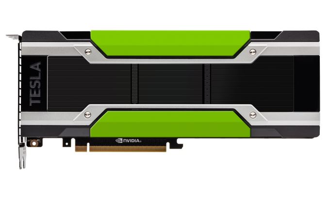
Kicking off this week in Frankfurt, Germany is the annual International Supercomputing Conference, better known as ISC. One of the two major supercomputing conferences for the year, ISC is commonly used as a backdrop for high performance processor announcements, and this year is no different. Starting things off this year is NVIDIA, who is taking to the show to announce the PCI Express version of the Tesla P100 accelerator.
We were first introduced to Tesla P100 back in April of this year, when NVIDIA announced it at their 2016 GPU Technology Conference. Based on NVIDIA’s new Pascal architecture and their 16nm GP100 GPU, Tesla P100 is a significant step up from the Tesla K/M series and their respective 28nm Kepler/Maxwell GPUs. Besides being a bigger-still GPU, P100 introduces a number of new features including larger caches, instruction level preemptive context switching, and double speed (packed) FP16 compute.
The initial version of the P100 announced at the time was NVIDIA’s highest performing version, a 300W board using NVIDIA’s new mezzanine connector, and shipping with 56 of 60 SMs enabled. The mezzanine connector marked a radical departure from traditional NVIDIA Tesla card designs, but also one that was necessary to facilitate NVIDIA’s high-speed point-to-point NVLink bus. However not every customer needs the features of NVLink or wants to build systems specifically for the mezzanine connector, and this is where the PCIe version of the card fleshes out the Tesla P100 lineup.
| NVIDIA Tesla Family Specification Comparison | ||||||
| Tesla P100 (Mezzanine) |
Tesla P100 (16GB) |
Tesla P100 (12GB) |
Tesla M40 | |||
| Stream Processors | 3584 | 3584 | 3584 | 3072 | ||
| Core Clock | 1328MHz | ? | ? | 948MHz | ||
| Boost Clock(s) | 1480MHz | 1300MHz | 1300MHz | 1114MHz | ||
| Memory Clock | 1.4Gbps HBM2 | 1.4Gbps HBM2 | 1.4Gbps HBM2 | 6Gbps GDDR5 | ||
| Memory Bus Width | 4096-bit | 4096-bit | 3072-bit | 384-bit | ||
| Memory Bandwidth | 720GB/sec | 720GB/sec | 540GB/sec | 288GB/sec | ||
| VRAM | 16GB | 16GB | 12GB | 12GB | ||
| L2 Cache | 4MB | 4MB | 3MB | 3MB | ||
| Half Precision | 21.2 TFLOPS | 18.7 TFLOPS | 18.7 TFLOPS | 6.8 TFLOPS | ||
| Single Precision | 10.6 TFLOPS | 9.3 TFLOPS | 9.3 TFLOPS | 6.8 TFLOPS | ||
| Double Precision | 5.3 TFLOPS (1/2 rate) |
4.7 TFLOPS (1/2 rate) |
4.7 TFLOPS (1/2 rate) |
213 GFLOPS (1/32 rate) |
||
| GPU | GP100 | GP100 | GP100 | GM200 | ||
| Transistor Count | 15.3B | 15.3B | 15.3B | 8B | ||
| TDP | 300W | 250W | 250W | 250W | ||
| Form Factor | Mezzanine | PCIe | PCIe | PCIe | ||
| Cooling | N/A | Passive | Passive | Passive | ||
| Manufacturing Process | TSMC 16nm FinFET | TSMC 16nm FinFET | TSMC 16nm FinFET | TSMC 28nm | ||
| Architecture | Pascal | Pascal | Pascal | Maxwell 2 | ||
NVIDIA will be shipping two versions of the PCIe Tesla P100. The higher-end PCIe configuration is essentially a downclocked version of the original P100 on a PCIe card. In this case we’re looking at the same 56-of-60 SMs enabled, only with a boost clock of 1.3GHz rather than the original P100’s 1.48GHz. This puts theoretical throughput at 9.3 TFLOPs for FP32 and 4.7 TFLOPs for FP64, versus 10.6 TFLOPs and 5.3 TFLOPs respectively for the original P100. The change in clockspeed is to accommodate the lower TDP of the PCIe card; whereas the mezzanine cards are 300W, the PCIe cards are 250W, which is the same TDP as past generation Tesla PCIe cards. Shipping with the same TDP means that these PCIe cards can be used as drop-in replacements for older Tesla cards, since they have the same power and cooling requirements.
Meanwhile on the memory side of matters, the higher-end card ships with the full 16GB of HBM2 enabled. Clockspeeds haven’t been dialed back here at all, so it’s still 1.4Gbps HBM2 in a quad package configuration, allowing for 720GB/sec of bandwidth (both with and without ECC).
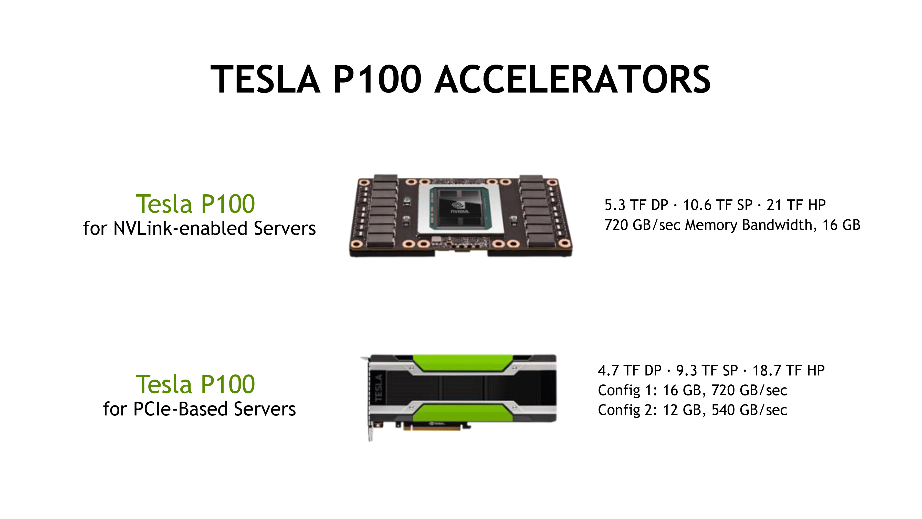
It’s on this latter point that the lower-end version of the PCIe Tesla P100 further changes things. The lower-end card ships with the same GPU clockspeeds and overall compute throughput, but it cuts the amount of memory and the memory bandwidth by 25%. This brings the total memory capacity down to 12GB, and the total memory bandwidth down to 540GB/sec. The L2 cache, which is directly tied to the memory controllers, is also reduced from 4MB to 3MB. NVIDIA has previously offered multiple tiers/prices of high-end Tesla cards – though usually under different model numbers to make them easier to differentiate – so having multiple PCIe cards is not unusual for the company.
Not explicitly said by the company (but is clear from the specifications) is that this is meant to be a salvage part for GP100. Because of the level of integration required by HBM2 memory, GP100 packages have to be fully assembled with their interposer and HBM2 ahead of time. This means that any problems with the package are permanent, and NVIDIA has to either toss or salvage the package. The lower-end PCIe card gives them the option of the latter; if a package comes out with a faulty HBM2 stack, interposer link, or HBM2 memory controller, then NVIDIA can disable the bad HBM2 stack and sell it rather than tossing it entirely.

Both of these cards are going to be targeted at customers who either don’t need NVLink, or need drop-in card upgrades for current Tesla cards. The lack of NVLink will impact performance to some extent in multi-card systems, but it’s going to be heavily dependent on the workload. For workloads that don’t require a lot of high-speed communication between GPUs, then the impact will be minimal, which would make the PCIe version a good, conventional fit for those customers.
Along with releasing the specifications, NVIDIA has announced that the PCIe Tesla P100 will be available in Q4 of this year. Given the additional hardware required to house the original mezzanine version of the P100 and the fact that NVIDIA uses those boards for their own DGX-1 server box, I suspect we’re going to see that the PCIe Tesla P100 will be the first P100 available in non-NVIDIA systems. Do note however that pricing for the PCIe cards has yet to be announced.
Finally, buried in the PCIe Tesla P100 announcement, NVIDIA has also reconfirmed that the Piz Daint supercomputer upgrade project is on schedule for later this year. The Swiss National Supercomputing Center will be doing a drop-in upgrade, replacing the supercomputer’s 4,500 Tesla K20X cards with Tesla P100 PCIe cards. This will be, to our knowledge, the first Pascal P100 based supercomputer to come online once the upgrade is completed.
Software Updates: DIGITS 4, cnDNN 5.1, & GIE
Along with the PCIe Tesla P100 announcement – though not strictly related to it – NVIDIA is also announcing some software updates to components of their Deep Learning SDK, the company’s collection of various software libraries and tools.
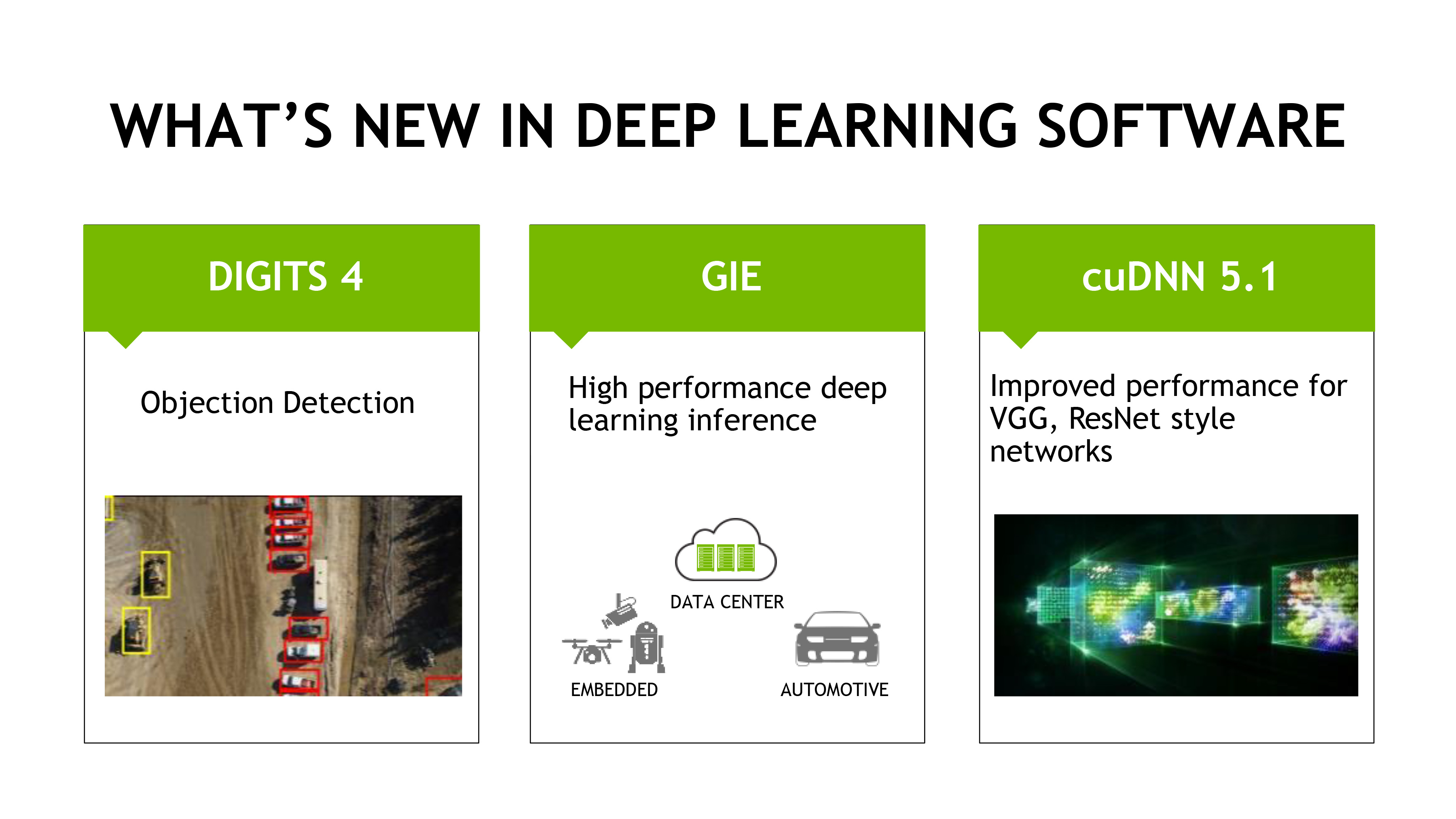
Set to arrive in the near future, both cuDNN and DIGITS are receiving upgrades. Version 5.1 of cuDNN is a minor update to deliver performance improvements for ResNet style networks. Meanwhile DIGITS version 4 is more significant, with NVIDIA adding object detection/recognition functionality to their neutral network training system.

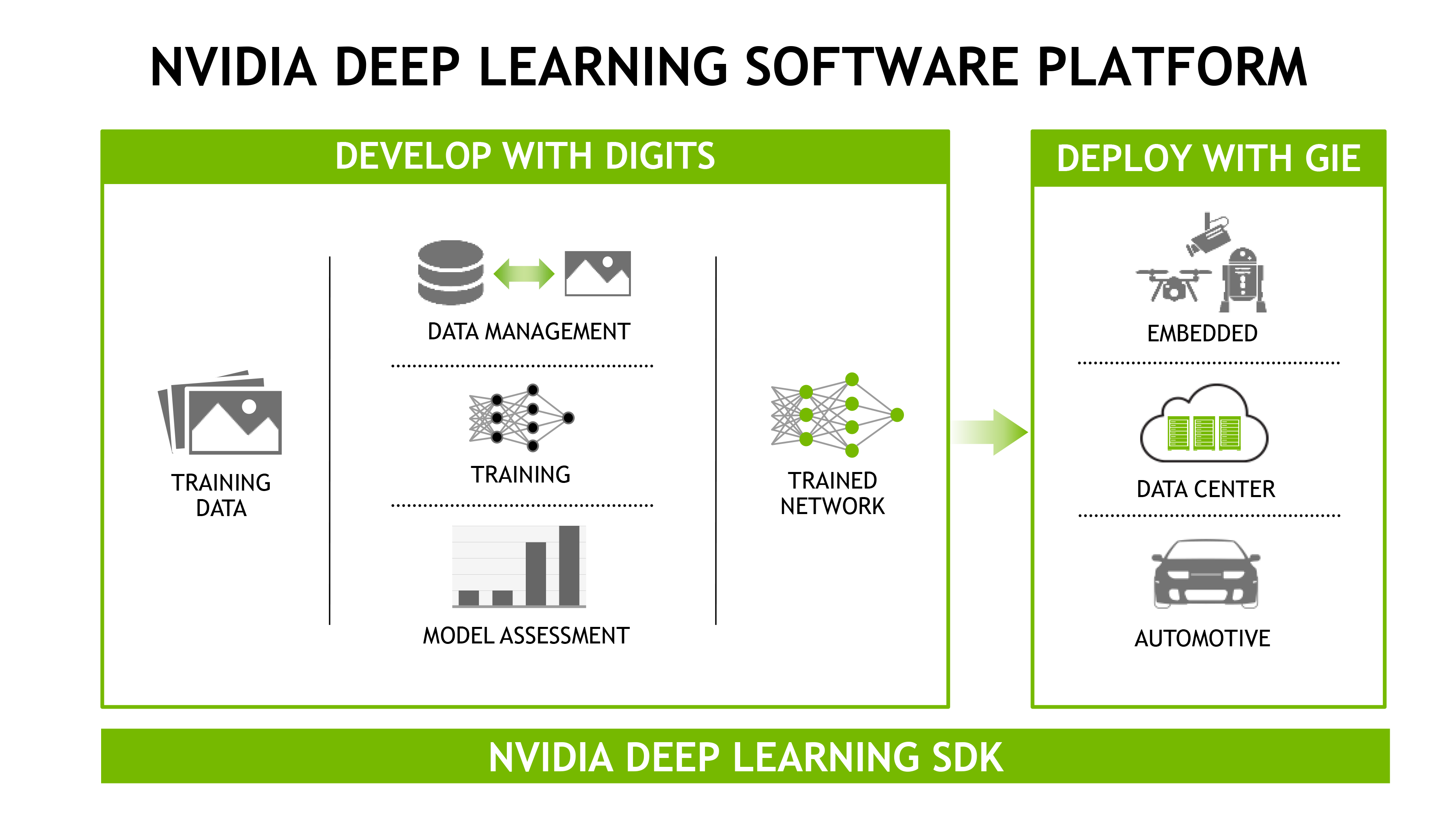
DIGITS 4 is also specifically designed to go with NVIDIA’s previously revealed GPU Inference Engine (GIE) software package, which was announced back at GTC 2016. As NVIDIA extends their efforts to get into deep learning/neural networks, DIGITS’ object detection functionality aligns with NVIDA’s other efforts, allowing developers to actually use (run inference with) their DIGITS-powered neural networks. The use cases for Drive PX2 and the Jetson TX1 board are very much rooted in real-world semi-autonomous devices, while NVIDIA expects object detection to be a big deal for Tesla M4 customers who are doing video analysis.


56 Comments
View All Comments
utroz - Monday, June 20, 2016 - link
Yes what about the FM2+ Excavator X4 845 analysis? Or are you "waiting" on the AM4 version Bristol Ridge?? Come on guys..ianmills - Monday, June 20, 2016 - link
Sometime before the rapture. Have faith my son!shabby - Monday, June 20, 2016 - link
And the 1070 review?Ryan Smith - Monday, June 20, 2016 - link
Yes, and the 1070 review.kael13 - Monday, June 20, 2016 - link
Where's that Retina Macbook Pro review, huh? ;PI kid, I kid. Say, are you hiring?
HighTech4US - Monday, June 20, 2016 - link
Quote: The GTX 1080 review will be posted.and that will be when exactly?
Beararam - Monday, June 20, 2016 - link
Risk becoming irrelevant when you wait so long. Might as well review the 950 too, if we're talking about reviewing cards that everyone site save this one has already reviewed.TheJian - Monday, June 20, 2016 - link
I really hope you guys don't plan on reviewing ANY AMD cards for at least a month after release just like 1080/1070. How much does AMD pay to stop/delay an NV review these days Ryan? ;) The first die shrink in ages and it takes more than a month to get a card from a shop or user etc? Really? Anandtech Broke all the sudden? NO friends to loan a card in PC shops etc? I'm guessing polaris reviews hit the second NDA goes up...LOL. AMD portal site...UGH. Is there another major site on the web WITHOUT a review of 1080? Most places have MULTIPLE reviews up now. Heck, hardocp has OC reviews comparing the founders 1080/1070. They are re-reviewing cards now sort of...ROFL. 1070 original review went up a 3 weeks ago (and a preview before that too), never mind the 1080's. They already had a 1070 oc review also, and now testing with new patches for the 1080/1070 OC comparison review (for dx12). So...Holy crap guys. One week is bad. One month is ridiculous. More than that and it's hard not to say AMD Portal site in the same sentence, especially when so many reviews, re-reviews, new patches/OC reviews etc are up. Guru3d has nearly a dozen different 1080/1070 articles (reviews of 3-4 cards each, frame pacing review, 2 way sli)...I mean c'mon. I don't know how many writers Hilbert has, but he is the ONLY name on all of them...LOL."Anyhow, we’ll be back later this week with our full review of the GeForce GTX 1080, so be sure to stay tuned."
So we can expect a review about Q4? LOL. It better take you 5+ weeks to get up AMD reviews :(
So POSTED when exactly? What about 1070? Pffft...Too harsh? At this point, if you don't expect flak, you're not living in reality. You are a hardware review site right? First gpu shrink in literally YEARS, and it only merits a preview. Hmm..
Luminair - Monday, June 20, 2016 - link
which chart has the typo?this one? http://www.anandtech.com/Gallery/Album/4926#12
or this one? http://www.nvidia.com/object/tesla-p100.html
ImSpartacus - Monday, June 20, 2016 - link
If both the pcie p200 and pcie p100 had the same 16gb of vram, then they would be identical.