AMD Teases Radeon RX 480: Launching June 29th For $199
by Ryan Smith on May 31, 2016 10:00 PM EST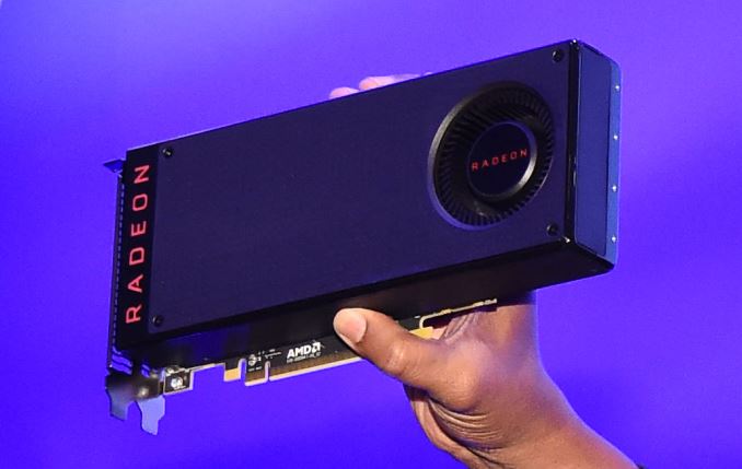
Kicking off at this moment is AMD’s Computex 2016 keynote. The company has multiple announcements scheduled this evening, but we’re going to jump right into an area that has been of extreme interest for many of our readers: GPUs.
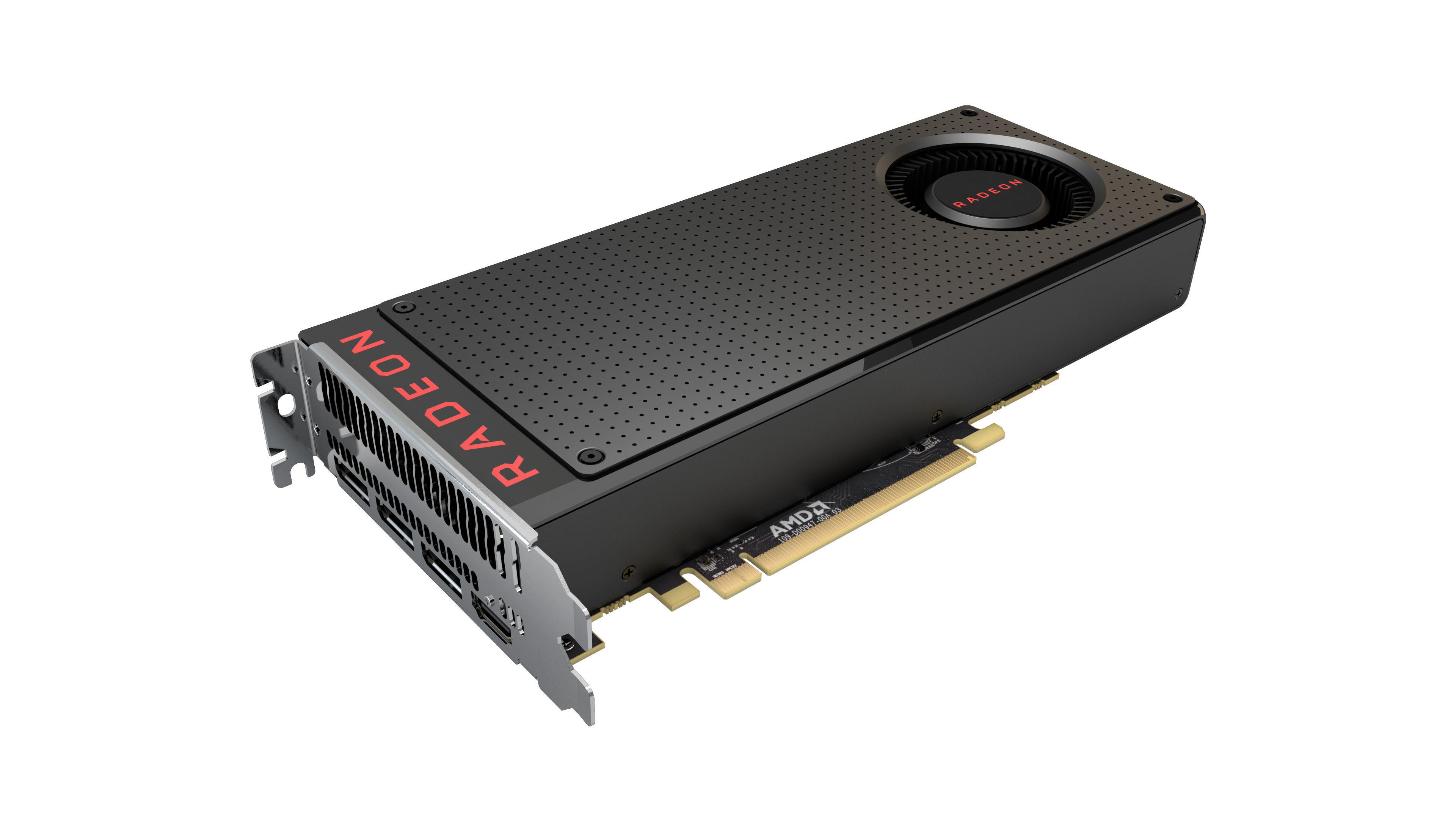
Ahead of this evening’s event, AMD sent out an email to the press teasing the first of their discrete Polaris architecture based cards. Called the Radeon RX 480, AMD has unveiled much of the product’s specifications, but also its price and availability. When the card hits the streets on June 29th, it will be starting at the crucial mainstream battleground price point of $199.
| AMD Radeon GPU Specification Comparison | ||||||
| AMD Radeon RX 480 | AMD Radeon R9 390X | AMD Radeon R9 390 | AMD Radeon R9 380 | |||
| Stream Processors | 2304 (36 CUs) |
2816 (44 CUs) |
2560 (40 CUs) |
1792 (28 CUs) |
||
| Texture Units | (Many) | 176 | 160 | 112 | ||
| ROPs | (A Positive Integer) | 64 | 64 | 32 | ||
| TFLOPs (FMA) | >5 TFLOPs | 5.9 TFLOPs | 5.1 TFLOPs | 3.5 TFLOPs | ||
| Boost Clock | >1.08GHz | 1050MHz | 1000MHz | 970MHz | ||
| Memory Clock | 8Gbps GDDR5 | 5Gbps GDDR5 | 5Gbps GDDR5 | 5.5Gbps GDDR5 | ||
| Memory Bus Width | 256-bit | 512-bit | 512-bit | 256-bit | ||
| VRAM | 4GB/8GB | 8GB | 8GB | 2GB | ||
| Transistor Count | ? | 6.2B | 6.2B | 5.0B | ||
| Typical Board Power | 150W | 275W | 275W | 190W | ||
| Manufacturing Process | GloFo 14nm FinFET | TSMC 28nm | TSMC 28nm | TSMC 28nm | ||
| Architecture | GCN 4 | GCN 1.1 | GCN 1.1 | GCN 1.2 | ||
| GPU | Polaris 10? | Hawaii | Hawaii | Tonga | ||
| Launch Date | 06/29/16 | 06/18/15 | 06/18/15 | 06/18/15 | ||
| Launch Price | $199 | $429 | $329 | $199 | ||
First off, the RX 480 will include 36 CUs. If we assume 64 stream processors to a CU – the GCN standard – then this brings us to 2304 SPs. AMD has not named the specific Polaris GPU being used here, but given the CU count I believe it’s reasonable to assume that this is a Polaris 10 SKU, as I’ve already seen Polaris 11 and it’s a very small chip better suited for notebooks.
AMD also revealed that the card would offer over 5 TFLOPs of compute performance. Given what we know about the CU count, this allows us to estimate the GPU clockspeed. This puts the lower bound of the GPU clockspeed at 1.08GHz and an upper bound (6 TFLOPs) at 1.3GHz, which would be in the range of 10-30% higher clocked than comparable Radeon 300 series cards.
In terms of raw numbers this puts the RX 480 just shy of the current Radeon R9 390. However it also doesn’t take into account the fact that one of the major focuses for Polaris will be in improving architectural efficiency. I would certainly expect that even at the lower end of clockspeed estimates, RX 480 could pull ahead of the R9 390, in which case we’re looking at a part that would deliver performance between the R9 390 and R9 390X, with final clockspeeds and architectural efficiency settling just how close to R9 390X the new card gets.
On the memory front the card is equipped with 8Gbps GDDR5, running along a 256-bit memory bus. This is the typical bus width for AMD x80-series cards, and the high clocked 8Gbps GDDR5 means that we’re looking at a total of 256GB/sec of memory bandwidth to feed the RX 480’s GPU. AMD’s partners will be offering both 4GB and 8GB cards, and for the purposes of this teaser I assume that pricing information will be for the 4GB card, with 8GB serving as a premium option.
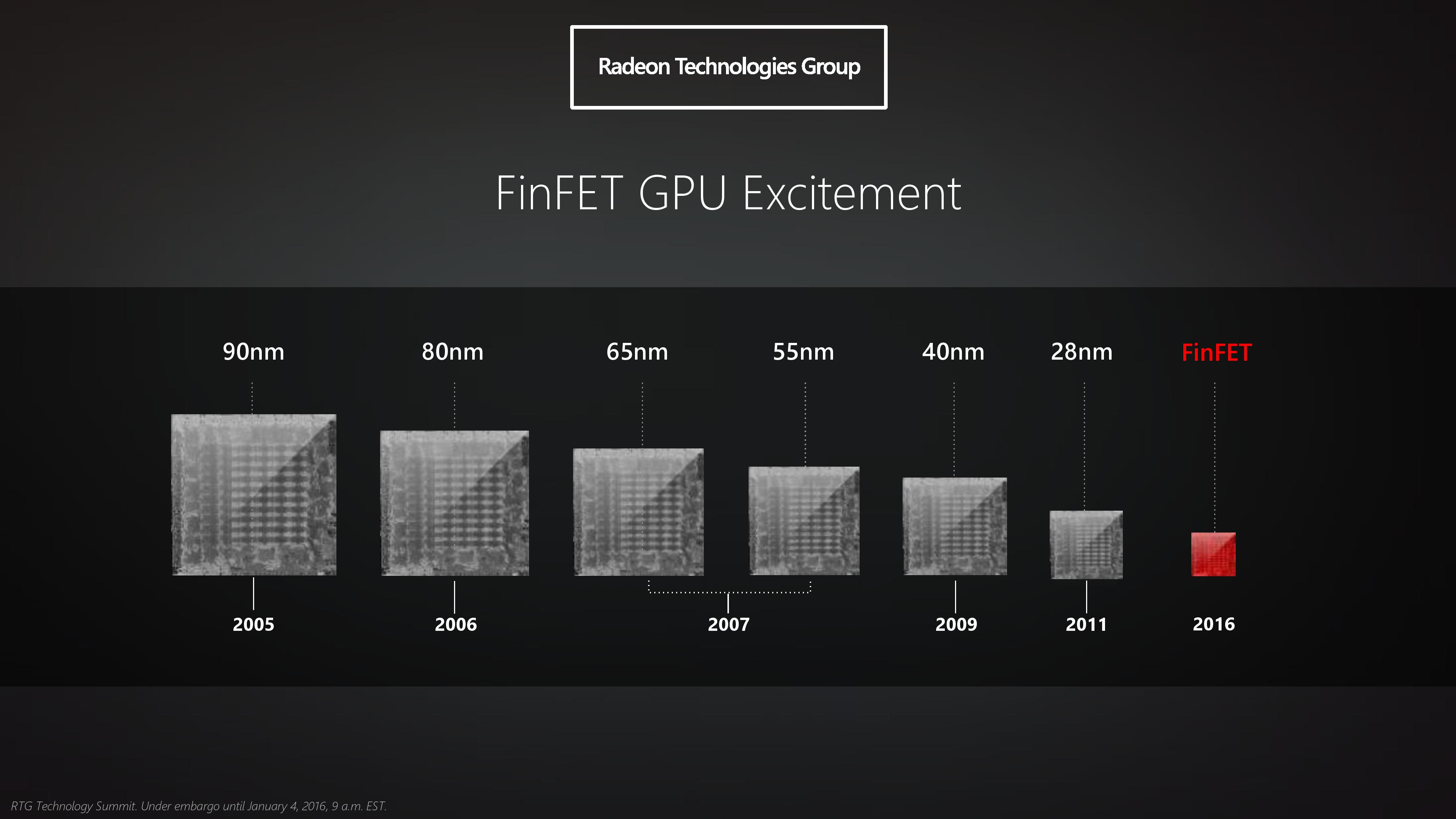
Finally, AMD has also revealed the TDP for the RX 480, stating that it will be a 150W card. As Polaris is built on 14nm FinFET, we’re seeing first-hand the benefits of finally making the long-awaited jump off of 28nm, as this means we’re looking at Radeon R9 390 series performance in a card that, on paper, consumes only a bit more than half the power. This also puts the RX 480 right in the sweet spot for mainstream cards, as 150W has traditionally struck a good balance between performance and power consumption that allows for a fast card that doesn’t require aggressive cooling, and is more compatible with OEM computer vendor case & cooling designs.
Cementing its place as a mainstream card, the RX 480 pricing will start at $199. This is an aggressive and heavily fought over price point that has traditionally defined the mainstream segment, attracting buyers who want great 1080p gaming performance that sub-$150 value cards can’t offer, without moving up to more expensive (and power hungry) $300+ cards. In this sense the RX 480 is a direct replacement for the R9 380, AMD’s Tonga-based card that hit the market roughly a year ago at the same price. Going by the raw numbers alone, RX 480 would be 40% (or more) faster than the R9 380.
Meanwhile I won’t speculate too much on the competitive market from a teaser, but it’s worth noting that this is nearly half the price of NVIDIA’s currently cheapest Pascal card, the GeForce GTX 1070. Interestingly both cards have the same 150W TDP, but looking at the throughput figures it does not look like RX 480 is meant to offer quite as high performance as NVIDIA’s card.


Moving on, along with teasing the RX 480’s specifications, AMD’s teaser also laid out their marketing plans for the card. We’re previously talked about how both Oculus and Valve/HTC were encouraging developers to treat VR like a fixed platform, and setting minimum hardware specifications to go along with that. On the AMD side those specifications called for a Radeon R9 290, which the RX 480 should be able to beat.
As a result AMD is planning on heavily promoting the VR aspects of the RX 480, as it brings the necessary performance down from a 250W, $300+ card to a 150W, $200 card. In fact AMD is claiming that VR performance will be closer to $500 video cards, in which case we’d be looking at performance closer to the Radeon R9 Nano, a Fiji based card.
With all of that said, the video card is just one component in the total price of a VR system – you still need the headset – but on the PC side it has also been the most expensive component. Consequently, AMD sees cheaper video cards that offer good VR performance as being important to bringing down the total price of a VR-ready system, and will be promoting the RX 480 as the prescription for entry-level VR needs. From a business perspective, AMD is ultimately expecting VR to be a fast-growing market, so the company wants to make sure they don’t miss out and have more VR-capable cards on the market as quickly as they can.
Along those lines, AMD’s release also makes note that at least one model will be “both HTC Vive Ready and Oculus Rift certified,” though no further details are being offered at this time. Whether this is just a certification matter or if there’s going to be something special about this model (e.g. connectors) is open to speculation.
Finally, now that they’ve revealed the price and much of the specifications of their first Polaris card, AMD is also releasing more details on their overall development and market positioning strategy with Polaris. As AMD has hinted at in the past, Polaris is being specifically developed for and aimed at the mainstream market. AMD wants to recapture lost market share – especially in laptops – and the large mainstream market is seen as the best way to do that. AMD is calling this their “water drop” strategy, and I expect we’ll hear a bit more about it tonight, including the meaning behind the name.
And with all of that said, it looks like we’re going to have a lot of AMD to talk about on June 29th. So until they, stay tuned.
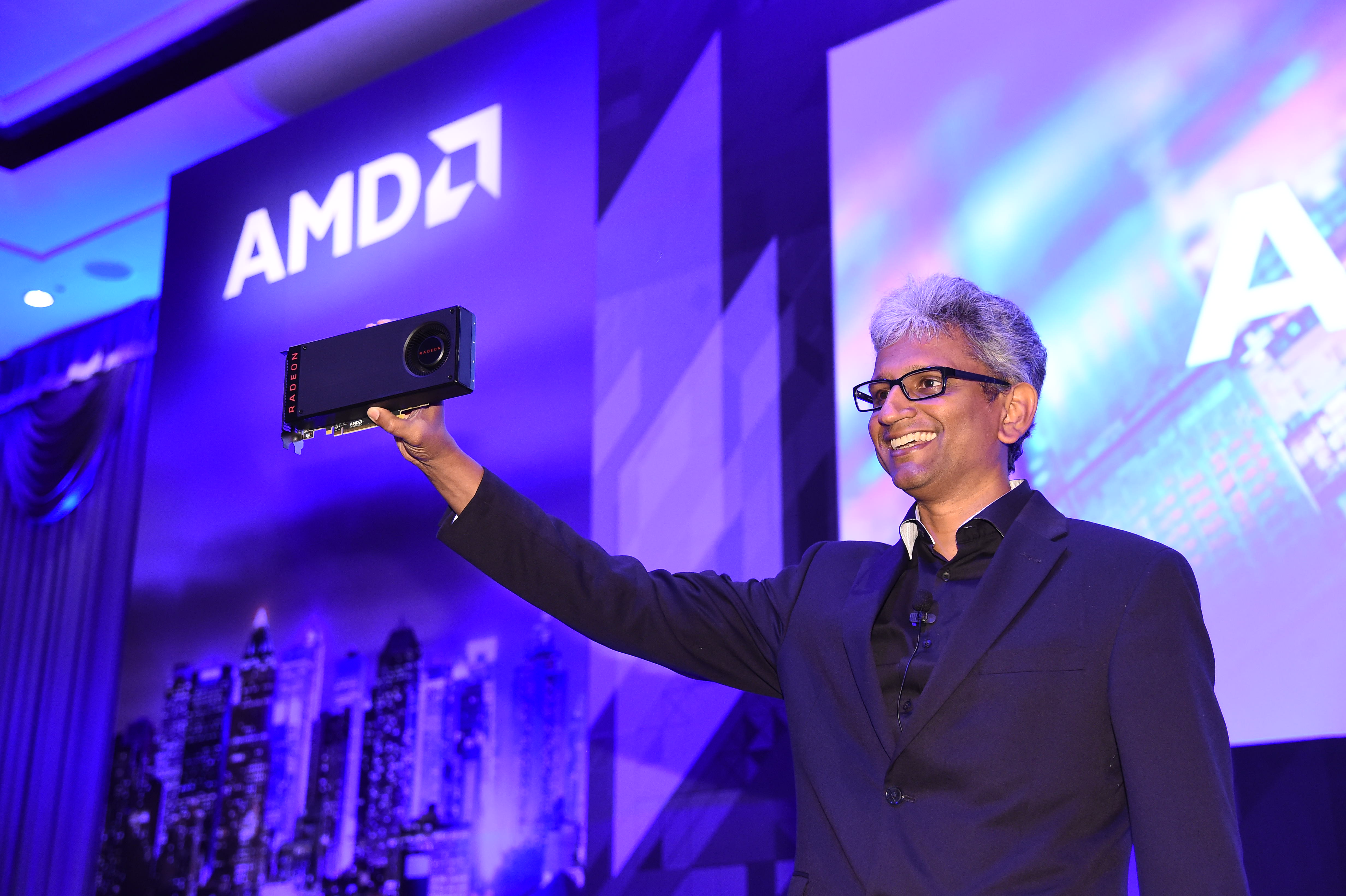
Above: AMD SVP & Chief Architect Raja Koduri, Who Is Very Happy That Polaris Is About To Launch


377 Comments
View All Comments
Ranger1065 - Wednesday, June 1, 2016 - link
Oh dear. With no sign of Chizoo, I hoped Nvidia trolls were on the decrease @ Anandtech.Zingam - Wednesday, June 1, 2016 - link
I agree... I prefer cheaper! :)gilmour - Wednesday, June 1, 2016 - link
Pretty sure some variation of this card will be my next purchase due to price and my performance needs but still disappointed in the specs that were shown.Considering the massive difference in clock speeds the GTX1070 can do at 150W it's very surprising how low the RX480 is at 150W.
Either the specs shown are still concealing real clock speeds and power draw and are better than shown, or the RX480 is a low end Polaris 10? part and there is a lot of headroom to release faster 480 and higher specc'ed 490 parts albeit with increased power draw.
Still seems Nvidia did some impressive engineering to get the clock speeds, performance and power draw at the levels they did, AMD maybe not quite so good.
beginner99 - Wednesday, June 1, 2016 - link
You can't compare TDP from NV and AMD. NV usually greatly understates TDP as was the case with 970 and 980. In real games the power use difference of whole system between a 970 and 290 was much less than the difference in TDP.Yojimbo - Wednesday, June 1, 2016 - link
TDP is not a measure of average power consumption. The TDP rating indicates the maximum sustained heat the chip is allowed to dissipate in real world usage, or put another way, the minimum heat the cooling system must be able to dissipate. If NVIDIA were to "greatly understate TDP" then their cards would be burning up left and right because their cooling systems wouldn't be able to keep up.If a card were to be consistently closely approaching its TDP across a wide range of uses then I think that card would probably be TDP bound. If one card is far from its TDP in a particular sustained real world use case, then there must be some other real world use case where it uses a lot more power, because otherwise the TDP claimed for the card could be lowered.
As far as what you said about the GTX 970 in comparison to the R9 290, it seems to me that you probably saw figures in just a small number of use cases. But if the 970 really is able to more consistently approach its TDP over an average of a large range of uses it seems to me that it implies the underlying architecture of the GTX 970 is more balanced, because there must be more extreme outliers for the R9 290 to require its TDP to be upped for those cases.
Regardless, the R9 290 consistently used significantly more power than the GTX 970.
Yojimbo - Wednesday, June 1, 2016 - link
An interesting thing I've noticed is how much NVIDIA's transistors per core count has gone up from Kepler to Maxwell and also from Maxwell to Pascal while AMD's transistors per core count has been relatively flat from 1st through 3rd generation GCN. I wonder what the transistors per core situation is for 4th gen. GCN.ajlueke - Wednesday, June 1, 2016 - link
Well, in Maxwell to Pascal you have actually changed process nodes, so you expect the number of transistors that can be placed on a die of the same size to increase. Now from Kepler (GTX 680) we went from 3.5 billion transistors to 8 billion in Maxwell 2 a 128% increase, all on the 28 nm process. While, AMD went from the 4.3 billion transistors in the HD 7970 (GCN 1) to 8.9 billion in the R9 Fury X (GCN) and increase of 107% all on the 28 nm process. Doesn't seem that different to me.Yojimbo - Wednesday, June 1, 2016 - link
I'm not talking about transistors per die area, but transistors per compute core (CUDA core as NVIDIA calls it). What that means is that NVIDIA has been using a greater percentage of the total transistors for cache, register files, ROPs, schedulers, and the like, and a lesser percentage on ALUs. But they have been getting greater efficiency out of their architectures by doing so.pashhtk27 - Wednesday, June 1, 2016 - link
Finally a card that I can dream of buying, something that won't make the poor me feel too bad investing on.If it can really offer gtx970 level performance, I'm in. Looking forward to release and benchmarks.
Will make a nice combo with egp docks when cheaper ones come out.
webdoctors - Wednesday, June 1, 2016 - link
I have the same thought/question. How does this card compare to the 970 which is now going for about the same price? Do we have a new $199 king?