Samsung Begins To Produce DDR4 Memory Using '10nm Class' Process Tech
by Anton Shilov on April 7, 2016 1:00 PM EST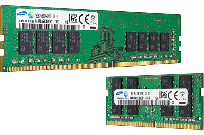
Samsung Electronics has started to manufacture DDR4 memory using its new '10nm class' production technology. '10nm class', by definition, implies sub-20nm but without fully disclosing the methodology, similar to the first sub-20nm NAND production that used 1x/1y terminology. By using a sub-20 nm fabrication process, this typically helps a company make ICs/DRAM cheaper, faster and more energy efficient, depending on the process complexity. In this case, Samsung continues to use ArF (argon fluoride) immersion lithography tools with quadruple patterning to make its latest memory, which indicates a very high complexity of the new process tech. What is also important is that the new DRAMs feature Samsung’s new memory cell structure.
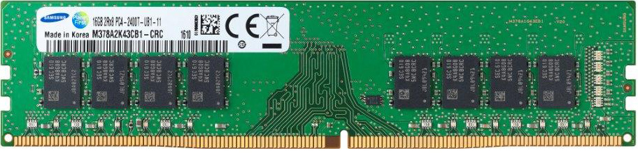
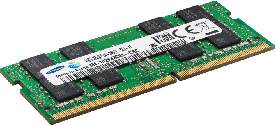
In the news today, Samsung’s new DDR4 memory chips are produced using 10nm-class manufacturing technology, have 8 Gb capacity, and can operate at 3200 Mbit/s data rate (DDR4-3200). In addition, the new DRAM devices are reported to consume 10 – 20% less power than equivalent DDR4 memory ICs made using a 20 nm fabrication process, based on tests conducted by the memory maker. Finally, Samsung can produce 30% more 8 Gb chips on a single 300 mm wafer thanks to the new manufacturing technology, which will lower their costs once their yields match those of current-gen chips due to having more chips per wafer.
Samsung does not disclose many details about its production process, such as its smallest half-pitch size (which gives actual names to DRAM manufacturing technologies, such as 20 nm or 25 nm). What we do know is that the new tech stacks very narrow cylinder-shaped capacitors on top of transistors, which implies a new DRAM cell structure (4F2?). Manufacturers of memory have historically changed the structures of DRAM cells every five or six years, and each change represents a major technology challenge as the density changes. Samsung says that it has refined the dielectric layer deposition technology and enabled substantial performance improvements, which may mean that the new memory chips can have a higher clock-rate potential than Samsung’s existing DRAMs, or more units will pass the base tests. If this is the case, if we extrapolate, this may open doors to DDR4 memory modules with unprecedented data rates (e.g., higher than DDR4-4400). Nonetheless, use of quadruple patterning significantly increases the complexity of manufacturing, which may somewhat slow down the ramp up of the new memory ICs and cause delays in increased yield refinements.
Samsung claims that later this year it intends to use its 1x nm manufacturing technology to make LPDDR memory with increased capacity, which should help makers of smartphones, tablets and notebooks boost the amount of DRAM inside their devices or reduce pricing.
Use of the sub-20 nm process technology to produce 8 Gb DDR4 chips should make such DRAM ICs cheaper (eventually), which will help PC and server makers to install more memory without increasing prices of their products. At press time, one 8 Gb DDR4 chip costs $4.688, according to DRAMeXchange. By contrast, a 4 Gb DDR4 IC is priced at $1.672. Therefore, using low-capacity chips is still cheaper than using high-capacity DRAM devices. Meanwhile, if you are building servers, you might not have a choice but to utilize 8 Gb chips to create high-end memory modules (i.e., with 128 GB capacities). For that reason, for server manufacturers, Samsung’s new 8 Gb DDR4 chips should be useful.


Source: Samsung


36 Comments
View All Comments
Samus - Saturday, April 9, 2016 - link
Is he really wrong? Samsung has a habit of dishonesty with various marketing strategies. Instead of calling things what they actually are, they segment products into "class" i.e. 55" class TV, 4K class bluray/DVD up conversion, ultrabook class PC, 10nm/20nm class NAND/DDR4, etc.Come on Samsung what is it, is it "like 10nm" or is it 10nm. Just call it 15nm if that's what it is. It's no secret, just say wtf it is.
none12345 - Thursday, April 7, 2016 - link
In 2008 i bought 2x2 gigs for $46, in 2013 i bought another 2x2 gigs for the same computer for $72.You can currently buy 2x8 gigs for ~$55(cheapest on newegg as of this is 49). And ~$120 for 4x8 or 2x16 gigs.
So, it went up and then came back down again.
I remember back when $100 for megabyte(4x256k) was a good deal heh. And dont forget inflation. That would be $300 or so in todays dollars.
jjj - Thursday, April 7, 2016 - link
lol even you guys go with the 10nm class BS, it's 18nm everybody knows that, just say it as it is.frenchy_2001 - Thursday, April 7, 2016 - link
The "critical dimension" you quote does not represent much anymore either way.Since the difficulty of improving process and how late Extreme UV has been, all manufacturers are using multi-patterning and those "critical dimensions" have very different meaning for each (TSMC 16nm is not at the same scale as Samsung 14nm or Intel 14nm).
A more useful comparison would be for a whole chip (for memory) and getting memory density (bits/sq.mm). Between cell architecture and different node dimensions, this would be a better representation. Anandtech tried this for flash.
jjj - Friday, April 8, 2016 - link
The process is one thing, the density is another(cell size is the better metric anyway) and costs an entirely different matter. The topic here was the process.Concillian - Thursday, April 7, 2016 - link
Let's hope we have some new "Samsung Green" sticks for DDR4 like we did for DDR3.For those who don't remember they were inexpensive sticks of plain looking high latency DDR3-1600 that routinely OC'ed to 2133 or optionally lower speeds but extremely low latency.
extide - Thursday, April 7, 2016 - link
Oooh yes I have like 48+GB of that DDR3 "Samsung wonder ram" at home, in various systems.T1beriu - Thursday, April 7, 2016 - link
Pfffff... What's this 10nm BS?! This can't be true. Even Samsung admits it: "new DRAM devices are reported to consume 10 – 20% less power than equivalent DDR4 memory ICs made using a 20 nm fabrication process, based on tests conducted by the memory maker"This can't be real 10nm.
Kristian Vättö - Thursday, April 7, 2016 - link
It's 10nm-class i.e. 10-19nm. It's more or less an industry standard to report "X0nm-class" instead of the exact geometry, even though that isn't a secret.The quote in your comment says that the new 10nm-class DRAM devices consume 10-20% less power THAN similar devices on a 20nm process.
yuhong - Thursday, April 7, 2016 - link
Thinking about it, Intel seems to have outlawed x16 chips on DIMMs/SO-DIMMs making 4GB sticks impossible with 8Gbit DDR4. And of course, you know that single channel RAM is bad for AMD APUs such as Bristol Ridge. I wonder if 16GB of RAM will ever become mainstream on laptops.